")
52896WA Advanced Diploma of Civil and Structural Engineering (Materials Testing)
Investigation of the properties of construction materials, the principles which…Read more")
Graduate Diploma of Engineering (Safety, Risk and Reliability)
The Graduate Diploma of Engineering (Safety, Risk and Reliability) program…Read moreProfessional Certificate of Competency in Fundamentals of Electric Vehicles
Learn the fundamentals of building an electric vehicle, the components…Read moreProfessional Certificate of Competency in 5G Technology and Services
Learn 5G network applications and uses, network overview and new…Read moreProfessional Certificate of Competency in Clean Fuel Technology - Ultra Low Sulphur Fuels
Learn the fundamentals of Clean Fuel Technology - Ultra Low…Read moreProfessional Certificate of Competency in Battery Energy Storage and Applications
Through a scientific and practical approach, the Battery Energy Storage…Read more52910WA Graduate Certificate in Hydrogen Engineering and Management
Hydrogen has become a significant player in energy production and…Read moreProfessional Certificate of Competency in Hydrogen Powered Vehicles
This course is designed for engineers and professionals who are…Read more
")


This manual will give you a solid understanding in electronic terminology and symbols, as well as the construction and operation of common electronic components and the testing and repairing of printed circuit boards.
Revision 5
Website: www.idc-online.com
E-mail: idc@idc-online.com
IDC Technologies Pty Ltd
PO Box 1093, West Perth, Western Australia 6872
Offices in Australia, New Zealand, Singapore, United Kingdom, Ireland, Malaysia, Poland, United States of America, Canada, South Africa and India
Copyright © IDC Technologies 2011.
All rights reserved.
First published 2009.
All rights to this publication, associated software and workshop are reserved. No part of this publication may be reproduced, stored in a retrieval system or transmitted in any form or by any means electronic, mechanical, photocopying, recording or otherwise without the prior written permission of the publisher. All enquiries should be made to the publisher at the address above.
Disclaimer
Whilst all reasonable care has been taken to ensure that the descriptions, opinions, programs, listings, software and diagrams are accurate and workable, IDC Technologies do not accept any legal responsibility or liability to any person, organization or other entity for any direct loss, consequential loss or damage, however caused, that may be suffered as a result of the use of this publication or the associated workshop and software.
In case of any uncertainty, we recommend that you contact IDC Technologies for clarification or assistance.
Trademarks
All logos and trademarks belong to, and are copyrighted to, their companies respectively.
Acknowledgements
IDC Technologies expresses its sincere thanks to all those engineers and technicians on our training workshops who freely made available their expertise in preparing this manual.
Contents
1 Introduction to Troubleshooting 1
1.1 Troubleshooting Basics 1
1.2 Common Troubleshooting Techniques 5
1.3 Gaining Circuit Familiarity 8
1.4 Getting Prepared for Troubleshooting 20
1.5 Summary 21
2 Failure Analysis and Prevention in Electronic Circuits 23
2.1 Failure Symptoms 23
2.2 Failure Causes 25
2.3 Failure Types 26
2.4 Some Useful Terms in Failure 28
2.5 Summary 29
3 Device Troubleshooting – I 31
3.1 Tools for Servicing 31
3.2 Test and Measuring Instruments 36
3.3 Safety Issues – Test and Tagging of Portable Electrical Equipment 54
3.4 Summary 55
4 Device Troubleshooting – II 57
4.1 Testing of Passive Components 57
4.2 Testing of Semiconductor Devices 62
4.3 Testing Bipolar Transistors 63
4.4 Testing Other Active Components 65
4.5 Testing Diodes, Transistors and In-circuit Semiconductors Using Oscilloscopes 78
4.6 Switches 80
4.7 Safety Issues for Plugs, Sockets and Portable Appliances 82
4.8 Summary 83
5 Troubleshooting Digital Systems 85
5.1 Moving from Analog to Digital 85
5.2 Moving into the Digital Circuits 87
5.3 Typical Faults in Digital Systems 97
5.4 Digital Circuit Troubleshooters 99
5.5 Digital Integrated Circuits 106
5.6 Programmable Logic Device (PLD) and Memory Definitions 108
5.7 Practical Tips 112
5.8 Precautions 112
5.9 Summary 112
6 Power Supply and Subsystems Troubleshooting 115
6.1 Power Supply 115
6.2 Regulators 119
6.3 Switched Mode Power Supplies (SMPS) 123
6.4 Oscillators 125
6.5 Amplifiers 129
6.6 Troubleshooting of RS-232 Serial Data Standard 131
6.7 Troubleshooting Microprocessor Based Systems 134
6.8 Summary 138
7 Temperature as a Parameter for Testing, Signal Injection and Signal Tracing 139
7.1 Effect of Temperature on Electronic Circuits 139
7.2 Testing 142
7.3 Actual Troubleshooting 143
7.4 Signal Injection 144
7.5 Signal Tracing 147
7.6 Summary 149
8 Phenomenal Troubleshooting 151
8.1 Noise 151
8.2 Intermittent 158
8.3 Sources of Interference 159
8.4 Static Discharge 160
8.5 EMI/EMC and its Sources 160
8.6 Cross-Talk 164
8.7 Summary 167
9 PCB Testing and Soldering Techniques 169
9.1 What is soldering? 169
9.2 Process of Soldering 170
9.3 Soldering Tools 171
9.4 Solder and Flux 175
9.5 Component Forming 176
9.6 Temperature Range in Soldering 177
9.7 Component Replacement 178
9.8 Inspecting Solder Joint 179
9.9 Unsoldering Connections 180
9.10 Additional Soldering Tips 183
9.11 Additional De-soldering Tips 183
9.12 First Aid Steps 184
9.13 Printed Circuit Board 184
9.14 Troubleshooting of Surface Mounted PCBs 189
9.15 Testing and Troubleshooting with ATE 191
9.16 Summary 198
10 Maintenance and Safety Aspects 201
10.1 Do we need Maintenance? 201
10.2 Types of Maintenance 202
10.3 Aims of Maintenance 204
10.4 Advantages of Preventive Maintenance 204
10.5 Importance of Sound Maintenance Management 204
10.6 Maintenance Policy 205
10.7 Maintenance Organization 206
10.8 Maintenance Manuals 207
10.9 Safety Aspects 207
10.10 Summary 211
Appendix A – Question and Answers 213
Appendix B – Questions and Answers 241
Appendix C – Troubleshooting of Variable Regulated Power Supply 269
Electronic equipment can develop a wide variety of problems. The act of troubleshooting arises in order to make the problems disappear so that the equipment works as per the expectation. This introductory chapter provides an overview of troubleshooting processes and various troubleshooting techniques. It also emphasizes how to prepare and read a circuit diagram, as a first step for troubleshooting.
Learning objectives
- Understand how to prepare a circuit diagram
- Study of electronic equipment in brief
- Study the basic concepts of troubleshooting
- Understand the process of troubleshooting
- Study the techniques used in troubleshooting
- Understand how to start troubleshooting
- Know preliminary precautions
1.1 Troubleshooting Basics
In general, for any application, equipment is designed and manufactured to work trouble free within its specified limits during its useful time. However, sometimes there is a conflict between the expectations of the user and the performance of the instrument. Thus develops the need for troubleshooting and maintenance.
What is Troubleshooting?
Troubleshooting is the process of isolating and correcting a problem in malfunctioning equipment so that it returns to its expected performance level. The process of troubleshooting requires a systematic fault finding approach. Whenever a fault occurs, two things can happen:
- The equipment does not work at all
- The equipment works abnormally
The second type of fault can be further sub-divided into:
- Constant error or malfunctioning (exceeding absolute maximum rating)
- Intermittent errors (external noise pick-up, heat, shock, increase in humidity, etc.)
The basics which can be applied to troubleshooting are given below:
- Look for obvious possibilities. If there are no obvious faults, measure the power supply voltage. If it is not the correct value, don’t go any further until you find out why.
- Use symptoms whenever possible to zero in on the section at fault. If the symptoms do not get you to the trouble region, use a signal tracing or signal injection method. These methods are discussed in an upcoming chapter.
- Once you have zeroed in the on the troubled circuits, locate the defective component. Tough problems like closed loops, distortion, noise and intermittent, require special troubleshooting techniques.
- Make efficient use of the troubleshooting and test equipments. Specialized equipment that you build yourself can also be very useful.
- Digital and microprocessor circuits require special equipment and a few special techniques.
- When looking for faulty components, troubleshooting should involve the following steps:
- Make a measurement
- Compare the measured value with what you are supposed to get
- If the measured values do not match what you are supposed to get, find out why
- When you have located the defective component, replace the component professionally. For surface mount components, some newer techniques are required.
- You should be well informed with the operation of testing and troubleshooting equipment. The selection of test equipment depends on the amount of service and the type of service. Some of the popular test equipment are:
- Analog VOM
- Digital VOM
- Oscilloscope
- Logic Probe
- Logic Pulser
- Sine-wave generator
- Regulated DC power supplies
- Transistor testers
- Finally make sure that your work indicates high quality professional servicing. Experienced technicians often use a type of statistical approach for troubleshooting. For example, if there is some distortion in sound in a speaker, there can be several possible faults for the symptom. From experience the technician knows that a battery will fail more often than a transistor. So the battery would be checked and replaced first.
- It is usually easier to replace a battery than a transistor; ease of replacement is also a factor.
The following table shows a list of component failure in their order of probable occurrence:
Order of occurrence of component failure
| Order of occurrence of failure | Component |
| 1 | Mechanical and electromechanical devices such as relays, switches, plugs and sockets. |
| 2 | Components that get hot in their normal operation, like power amplifiers and rectifiers. |
| 3 | Electrolytic capacitors of small versions and those subjected to high voltage. |
| 4 | Active devices like transistors and SCRs. |
| 5 | Passive devices like resistors and capacitors. |
- As said earlier it is best to measure the power supply voltage first, when beginning troubleshooting. If the power supply voltage is not the correct value, nothing will work well in the circuit.
- A low power supply can cause failure to the circuit, which is not located anywhere near the supply. It is best to measure the power supply voltage while it is delivering current to the system. In battery operated equipment, the system should be energized when the battery voltage is being measured.
- An incorrect power supply voltage can damage a digital system. If a wrong power supply voltage is measured in a digital circuit, shut it down immediately. Then use your bench supply to energize the circuit and look for possible damage caused by the incorrect voltage.
- While measuring the power supply voltage with an analog meter, if you are not sure what value of voltage (or current) you are going to be measuring, then you have to start with the highest scale and work down.
The Troubleshooting Process
The process of troubleshooting comprises the following steps:
- Fault Establishment
- Fault Location
- Fault Correction
Let’s address these steps in brief:
Fault Establishment
It is important to establish the presence of a fault in equipment before taking any other action. In some cases a system may be reported faulty, but it could be a case of faulty operation or a system failure may be reported with either very little or misleading information. It is essential that a functional test, checking the system’s actual performance against its specification must be made and all fault systems must be noted.
It is also important to check the history of the equipment and repair and servicing work carried out earlier by any other person.
Fault Location
This involves pin-pointing the cause of the fault by studying the literature relevant to servicing, maintenance and repairs. The fault is located first in subsystem and then in a single component in the sub system.
Fault Correction
Fault correction consists in replacing or repairing the faulty component. This is followed by a thorough functional check on the whole system.

Troubleshooting Aids
Troubleshooting aids help in quickly analyzing a malfunction and taking corrective action. The following points are discussed in this aspect:
Tools
A basic set of tools and test equipment like multimeter and oscilloscopes are necessary. Sometimes specialized equipment are required, such as a high speed scope. The maintenance technician is required to have all this knowledge.
Documents
A complete set of documentation is a must. Most manufacturers supply the following documents with their manuals:
- Schematic document
- Circuit board illustration
- Circuit board location
- Power distribution diagram
- Circuit board interconnection diagram
- Fault tracing flowchart
- Diagnostic software
- List of replaceable parts
- List of special tools for servicing
Data Manuals
A good list of data manuals is essential. There are data books from all major component manufacturers which can be collected.
Thumb Rule in Troubleshooting:
- If the equipment is totally dead, then the problems are generally related to the malfunctioning of the power supply.
- If the equipment starts malfunctioning when it warms up, it can be due to the dryness of electrolytic capacitors. In this case they should be tested.
- The problems which come and go suddenly, intermittent problems are often due to bad connections. The reason for this can be a cold solder joint of internal or external connectors that need to be cleaned.
- Failures because of burnt, melting of the leads of components, cracking of the components and so on are identified by visual inspection and burnt smell.
1.2 Common Troubleshooting Techniques
The various troubleshooting techniques given below are used in the majority of electronic systems. The type of system being handled will decide which technique should be adopted.
Functional Area Approach
An electronic system comprises several functional parts such as power supplies, amplifier, signal converters, etc. When the system fails to give the expected performance, the problem could be in any of these functional areas. Therefore, it is essential to troubleshoot the system in order to isolate the fault to the failing functional area and then to the failing component. The logical approach of isolating a fault is through a process of elimination of the functional areas that are performing properly. Once a failure is isolated, further analysis of the circuitry within this area is carried out to isolate the malfunction to the faulty component. This functional area approach is also called the Block-Diagram approach to troubleshooting.
Split Half Method
In this technique, as the name suggests, the circuit is split in half and the output is checked at the half-way point in case of an absence of an output. This helps to isolate the failing circuit in the first or second part. When the faulty half is determined, the ageing circuit is split into half for further isolation of failure. This splitting is continued until the failure is isolated to one function or component.
The Half-split method is extremely useful when the system is made up of a large number of blocks in the series:
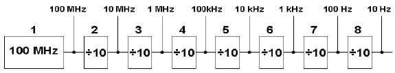
Split Half Method
Many electronic systems do not involve only series connected blocks. They may have feedback loops or parallel branches in a part of the circuit. Hence use of this method is rather restricted.

Divergent Path
Here the output from one block is fed to two or more blocks. In such systems, it is best to start by checking the common feed point. Alternatively if output is normal (at A or B in fig. 1.3), check after the divergence point. Conversely, if one output is abnormal, check before the common point. The most common example is that of the power supply circuit which supplies dc power to various subsystems in equipment.
Convergent Path
In a convergent path two or more input lines feed a circuit block:
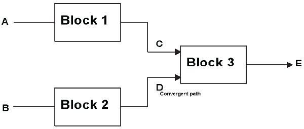
Convergent Path
In order to check such a scheme, all inputs at or before the point of convergence must be checked one by one. If any of the inputs is incorrect (at C or D in fig. 1.4), then the fault lies in that particular input circuit. If all are found to be correct, the fault lies beyond the convergent point. For example, if C and D are correct and there is no output at E, the fault lies in unit 3. But if input at C is faulty, the fault lies in block 1 or before that.
Feedback Path
The feedback loop usually corrects the output of some block with the input of an earlier block via some network called feedback network. Since the circuit behaves as a closed loop, any fault within the loop will appear as if all the output blocks within the system are at fault:
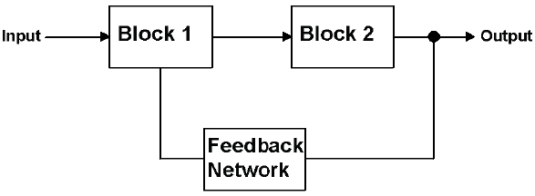
Feedback Path`
Before starting the troubleshooting of a system having feedback loop, the type of the feedback and its use should be well understood. Feedback paths are basically provided for the following functions:
- To modify circuit function —- Feedback loop is provided to modify the characteristics of the system. For example, automatic gains control system in a radio receiver.
- To sustain circuit function —- Feedback is totally essential for an output to exist. For example, an Oscillator circuit.
Having identified the type of feedback circuit, one can proceed as follows regarding locating the fault.
For the first type, i.e. modifying feedback, it may be possible to break the feedback loop and convert the system to a straight linear data flow. Each block can then be tested separately without the fault signal to be fed around the loop. In some cases instead of completely breaking the loop, the feedback can be modified at or near the point where it rejoins the main forward path. If the output appears normal, check the feedback path, otherwise, check the forward path.
For the second type, i.e. sustaining type, feedback is disconnected from the output and a suitable test signal is injected to check the performance of various circuit blocks.

Fault Location in Switching Path (rsk40)
If a system has switch-able parts and if the circuit function is found faulty in one position of the switch then throw the switch to another position. If the problem persists, check the switch in common circuitry. If the problem disappears with this action, check that the circuitry switched out.
1.3 Gaining Circuit Familiarity
A circuit diagram is a graphical representation of the interconnections of various components constituting the equipment. It is the most important document for the maintenance technician. Usually every assembly in electronic equipment is assigned an assembly number which appears on the circuit board and on the diagram. Commonly used symbols in electronic circuits are shown below in Figure 1.7.
The maintenance technician should be well versed with the circuit of the system before actually starting troubleshooting. A circuit diagram is the most important document for the technician. Many-a-time the circuit diagram of the system or equipment is not ready or not provided by the manufacturer. In that case, the technician has to prepare the circuit diagram. The circuit diagram makes the fault finding process easy.
Preparing a Circuit Diagram
The technician should be experienced enough to draw a circuit diagram. Usually, it is not recommended for larger systems. A larger system is broken into parts (subsystems) and then circuit diagrams for the smaller, suspected systems is drawn to trace the fault. The following points must be noted when preparing a circuit diagram:
- After identifying what is the type of fault, the very first thing to be done is to understand the functionality of the system. Split the system into a few functional blocks, which will make a functional working diagram.
- The components and their types are identified. The specifications of the components are notes taken from the manual or data book given with the equipment.
- Make a note of the interconnections of various subassemblies like power supply, PCB assembly, front panel, etc.
- The printed circuit board is removed. Usually individual boards can be removed in industrial systems as they are of modular construction for easy maintenance.
- First locate the components on the paper. Understand the PCB pattern. Place the PCB in front of strong light so that the PCB interconnections are clearly visible. If you look at the back of the PCB, then what you see is the mirror image of the connections as seen from the front. Now, make a sketch of the components and PCB pattern.
- Clearly differentiate between input and output. Start with the supply rail, not the common. Now draw the components connected to the supply lead. The ground or common lead will be easy to identify.
- Use your knowledge of the functional aspects of the equipment to draw out the stages. Power transistors will be either with the power supply circuit or in the output stage. If one stage gets a bit complicated try starting from another stage like input or output stages following the signal path.
- Now redraw the circuit in the conventional manner. After the initial attempt, the technician will be able to identify the nature of the circuit.
- Check if all the components on the card are in the sketch and check the polarities of the components.
- Always draw the sketch with pencil for easy correction.
Reading a Circuit Diagram
A circuit diagram is a graphical representation of interconnections of various components constituting the equipment. It is the most important document for the maintenance technician. Usually every assembly in electronic equipment is assigned an assembly number which appears on the circuit board and on the diagram. Commonly used symbols in electronic circuits are shown below:
Various Symbols in electronic circuits
Circuit symbols to DIN EN, NEMA ICS/ANSI/IEEE/CSA
(The following comparison of circuit symbols is based upon the following international/national specifications:
-IEC 60617 graphic symbol database (DIN EN 60617-2 to DIN EN 60617-12
-NEMA ICS 19-2002, ANSI Y32.2/IEEE 315/315 A, CSA Z99) 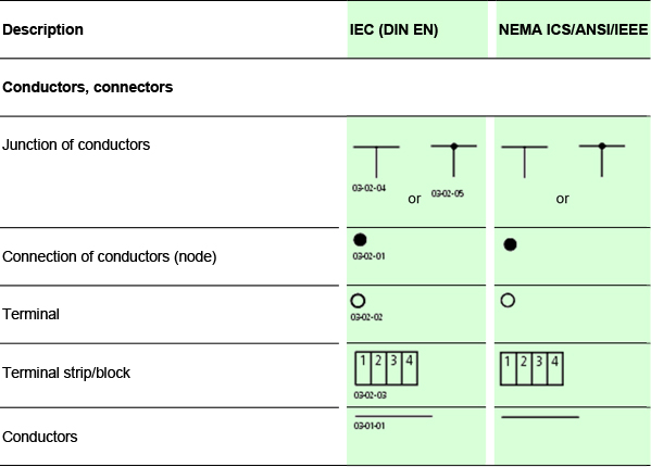


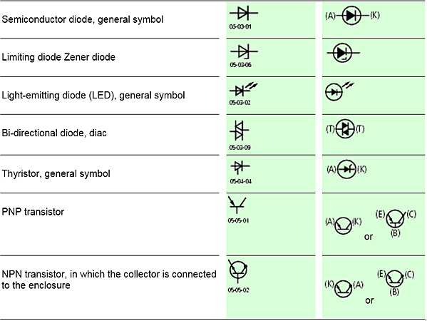
A circuit diagram illustrating some symbols is also shown below:

Electronic Circuit Diagram
The Making of an Electronic Circuit
An electronic circuit makes use of both active and passive components. These components are physically interconnected with each other to form any electronic circuit. There are three major techniques to interconnect the components. Let us have a brief overlook of these methods:
- Solder
- Wire-wrap
- Printed Circuit Board
Solder
This method makes use of a solder and a wire to interconnect electronic components. It is a very slow method and is very cumbersome if a large number of devices are to be connected.
Wire-wrap
This technique tightly winds a small gauge wire around a wire-wrap metal post or terminal. There are special wire-wrap metal post sockets for the ICs that have longer posts for wire-wrapping the wire. Also, special tools are needed for wrapping and un-wrapping the wire.
Printed Circuit Board (PCB)
This technique includes interconnections between points printed in metal on the non-conductive board. The circuit is printed on the board by a series of photographic and chemical procedures. Most of the equipment in practice make use of PCB. They are generally made for completely checked out and working boards, as it is difficult to make wiring changes on the PCB.
A Quick Glance at Electronic Equipment
There can be one or more circuit boards inside of electronic equipment. They are mounted inside a wooden or metallic cabinet with some arrangement of interconnecting the circuit boards. This arrangement is called Edge Connectors.
The purpose of edge connectors is to bring signals and powers to and from the circuit boards without having to connect a wire to the circuit board itself. This arrangement provides easy installation and removal of the circuit board in equipment:
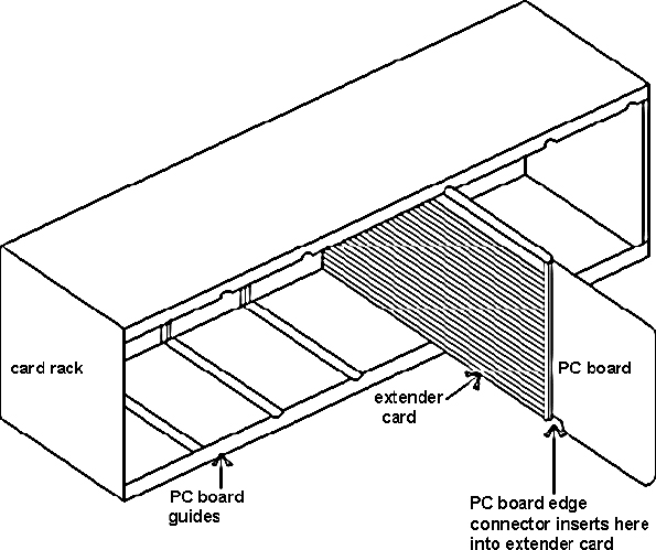
Electronic Equipment
Also inside of electronic equipment there is an assembly called card rack for the compact placement of the PCBs. But it is difficult to put a test probe on the circuit board for making any type of measurement or for troubleshooting. To eliminate this problem, special circuit boards called ‘extender cards’ are inserted into the card rack and the circuit board is extended into the extender card.
An extender card is just a wiring extension to make the circuit board accessible for testing.
Classification of System
In the literature, terms such as component, equipment or system have been used. The following table distinguishes between these terms:
Classification of System
| Serial Number | Nomenclature | Description | Example |
| 1 | System | Collection of equipment arranged to perform a function. | Television, Missile. |
| 2 | Equipment | Collection of components arranged to operate without the need for other components. | Radio Transmitter, the central part of a missile. |
| 3 | Assembly | Collection of components in a prescribed order not all of which have, as yet, been so arranged. | Terminal board with components parts attached. |
| 4 | Component | Collection of elements arranged in a prescribed order. | Resistor. |
| 5 | Element | A simple object which can not be further sub-divided. | Filament, a relay contact. |
1.4 Getting Prepared for Troubleshooting
Where do you start?
A close visual inspection is a good and quick start for troubleshooting. It gives a clue for problems such as burned spots and places where high voltage arc has occurred. A quick look to the circuit also gives an idea of the condition of fuses and circuit breakers.
The troubleshooting technician should collect the history of the system. He/she should know whether the problem had occurred before and what is the frequency of the occurrence of the problem.
On the basis of the knowledge of how the system works, the kind of failure can be detected. This would lead you to select the troubleshooting technique.
If the system is not producing the desired end result, look for what is doing it correctly. You can locate where the problem is not present so that you can then focus on another location for troubleshooting.
If the system has been having problems immediately after some kind of maintenance or other change, the problems could be linked to those changes.
After all, the choice of techniques and strategies for troubleshooting totally depends upon the technician. The following points would be helpful for effective troubleshooting:
- Familiarity with the equipment
- Analyzing possible causes of trouble
- Developing a general troubleshooting procedure
Preliminary Precautions
- Identify the mains power supply voltage and the maximum voltage that can be applied from the power source. The mains power supply voltage can be either 110 V, 60 Hz or 220 V, 50 Hz. Make sure that a protective ground connection by way of the grounding conductor is or is not provided.
- In order to avoid shock, the power cord must be plugged into a properly wired receptacle before connecting to the equipment’s input or output terminal.
- The service manual which is provided along with the equipment should be studied thoroughly before starting troubleshooting. The caution statements, warning statements and other information should be read carefully.
- Always disconnect the power to the equipment before removing the cabinet panels and before cleaning or replacing parts to avoid electric shock hazard.
- The circuit boards should be handled by edges to avoid inaccurate performance because of static charges, dirt, dust etc. Check the conditions of all external cables for splits, cracks, twists and so on
1.5 Summary
For the process of troubleshooting, preparing the circuit diagram is the initial and basic process performed by the maintenance technician.
The components can be physically interconnected to each other using solder, wire-wrap and printed circuit board methods.
Any electronic system consists of an element, component, assembly and equipment. All these parts together make a complete electronic system.
The troubleshooting process consists of fault establishment, fault location and fault correction.
Functional area approach, Split half method, Divergent path, Convergent path, Feedback path, Switching path are the common troubleshooting techniques. Which technique has to be applied totally depends on the type of system.
To start the process of troubleshooting, first the technician should have a close visual inspection of the system. He should understand the basic functionality of the system. Then he can proceed to analyze the cause of the trouble.
A well designed, well engineered, thoroughly tested, and properly maintained system should, ideally, never fail in operation. However, in practice it is observed that even the best design, manufacturing and maintenance efforts do not completely eliminate the occurrence of failures. There can be various causes and types of failures.
For the enhancement of system reliability, it is necessary that the design engineer understands the causes of failure, so as to trace the deficiency in the system. The primary concern is to identify the correct causes of failure and to decide on appropriate corrective action to assure higher system reliability.
Learning objectives
- Understand the technical meaning of failure
- Know the symptoms of failure
- Study the causes of failure
- Study Early Failure, Random Failure and Wear out Failure
- Know what is Failure Rate, Mean Time to Failure, Mean Time between Failure and Mean Time to Repair
2.1 Failure Symptoms
Failure
The reliability of equipment improves considerably when it is operated under certain favorable conditions (which may vary from equipment to equipment) such as operating the components well below the maximum ratings, subjecting the components to minimum vibrations and shocks, etc. In spite of all the favorable operating conditions, failures are seen to occur.
The frequency at which the failure occurs is termed as reliability of the system. The less is the occurrence of failure, the more is the reliability of the system.
Definition of Failure
Any equipment or a system may breakdown due to a faulty component. For each component or item, the properties that it must possess in the course of its use are listed.
A deviation in the properties of the component or item from prescribed condition is considered as a fault. A state of fault is denoted by the term failure.
Failure of equipment refers to its inability to perform its required function, such as when characteristics change to such a degree that it can not perform its specified level of performance.
The fundamental sources of failure include many aspects of design, material selection, material imperfections, fabrication and processing, assembly, inspection, testing, quality control, storage and shipment, service conditions, mechanical and chemical damage to system.
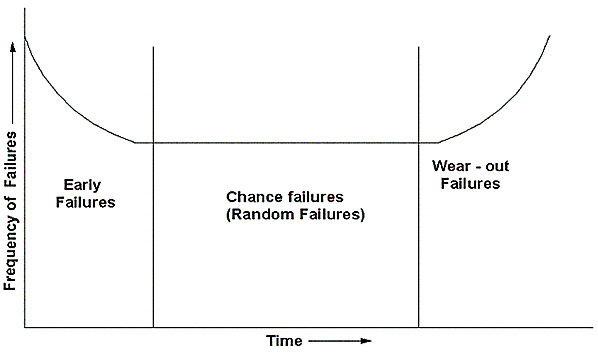
Failure Curve

Failure Curve)
The traditional bathtub curve in figure 2.1 indicates component life in three stages.
During the first stage, failure rate begins high and decreases rapidly with time. This stage is known as Infant Mortality Period and it has a Decreasing Failure Rate (DFR). The infant mortality period is followed by a steady state failure rate period, which is usually long. This period is known as random failure period or useful life of the equipment and this part of the curve being identified as normal operating life curve.
In the third stage where the curve ends, i.e. beyond the useful life period, there is a gradual increase in failure rate. This is a period of ageing and wears out with increasing failure rate.
Equipment Failure
Failures may be partial failures resulting from deviation in characteristics or parameters beyond the specified limits but not such as to cause complete lack of required function. If the characteristics deviate beyond the specified limits such as to cause complete breakdown of the required function, it is called as complete failure.
Failures can be anticipated by prior examination, whereas in some cases, it can be a sudden failure which could not be predicted on routine examination. A sudden and complete change in equipment performance is called as catastrophic failure.
These may be caused by an open circuit or short circuit failure which is irreversible.
Failures may also occur gradually and in a partial manner. Such a type of failure is referred to as degradation failure. These failures are encountered mostly with analog systems when some noise or disturbance is present.
Symptoms
Symptoms are useful to locate the general area of problem. The symptoms are sometimes described by the equipment owner or user. In an industrial electronic plant, it may be the foreman of the division who uses the equipment. In consumer electronic equipment, the description is often from the customer who owns the equipment.
The most reliable symptom analysis is given by the technician after energizing the equipment. Technicians know that certain symptoms in a system usually mean that a certain component has failed.
Symptoms are indeed a valuable guide for troubleshooting. However, one should avoid basing a complete troubleshooting procedure on the knowledge of symptoms alone. For example, distortion in radio’s output sound can be caused by different reasons such as low terminal voltage of aging battery, overuse of transistor, a tear on a speaker cone and so on.
An item is considered to have failed because of one of the following three conditions:
- When it becomes completely inoperable
- When it is still operable but is no longer able to perform its intended function satisfactorily, or
- When serious deterioration has made it unreliable for its continuous use, thus necessitating its immediate removal from service for repair or replacement
2.2 Failure Causes
For the enhancement of system reliability, it is necessary that the design engineer understands the causes of failures, so as to trace the deficiency. Equipment failures take place due to many reasons. The primary concern is to recognize the causes of failure and to take corrective action to achieve higher reliability. The causes can be classified as follows:
Design Deficiency
- Little engineering efforts and changes in design
- Improper choice of components
- Upgrading of a part
- Inadequate information on failure analysis of components
- Insufficient design criteria
- Insufficient prototype testing for meeting both reliability and performance specification
- Excessive heat development inside the equipment and lack of cooling
- Poor mechanical layout of components, assemblies and panels
Production Deficiency
- Imperfection in purchase of material for substandard manufacturer or company
- Unsuitable storage method and unduly long storage period of components
- Absence of training programmers to employ correct and effective production techniques
- Negligence in performing environmental tests like temperature cycling, operation of equipment at elevated temperature for specified period
- Lack of proper working environment, ill-ventilated, poor illumination and dusty assembly shops
- Lack of inspection of goods, sampling tests and inspection
- Insufficient testing and inspection of finished product
Processing Deficiency
- Incomplete or ambiguous specification, specification of unsuitable processing procedures
- Changes in the specification without complete evaluation
- Improper heat treatment, electroplating, welding
- Cold forming, machining, improper identification marking
Assembly Errors
- Undetected errors in assembly by the manufacturer or the purchaser
- Improper matching of various signals used or generated by the components on the terminal board at the time of assembly
- Improper prescribed order of the components collected on the terminal board
Careless Storage and Transport
- Undue long storage of equipment before its dispatch to the customer
- Improper packaging which may be unable to protect the equipment from corrosion or mechanical damage
- Excessive vibrations and mechanical shocks during transportation of equipment from manufacturer to the user
Improper Working Conditions
- Presence of abnormally severe conditions of speed, temperature, loading and lack of dust free areas, air-conditioned rooms
- Using the equipment without following manufacturer’s instructions, warnings and cautions
- Inadequate maintenance policy and after sale service by the manufacturer
- Usage of the equipment beyond its lifetime
- Aging of the equipment
- Poor operating ability of the equipment with the possibility of high degree of operator error
- Lack of preventive measures
2.3 Failure Types
During the complete life cycle of the operation of a system, failures are broadly classified into three categories as follows:
- Early Failure
- Random Failure
- Wear out Failure
Failure Types
Early Failure
- As the name suggests, errors occur during the early life of the system’s operation.
- These failures could be attributed to variation in manufacturing process and poor quality control techniques during production.
- The method of inspection and improper assembly of components may also lead to early failure.
- They are also known as Infant Failures. These can be eliminated by de-bugging or burn-in process.
- The testing procedure consists of monitoring system characteristics by simulating conditions of actual use.
- The weak and substandard components which fail early are replaced by good and tested components.
- Debugging is generally done prior to delivering the system to the user to ensure the detection and elimination of early failures.
Random Failure
- They are also known as chance failures and are predominant during the actual operation of the system.
- They occur at random, irregularly and unexpectedly.
- These failures are caused by sudden stress accumulations beyond the design strength of the component.
- It is highly unpredictable when the chance failures will occur, however they obey certain rules of behavior so that the frequency of their occurrence during sufficiently long periods is approximately constant.
- The phase during which only chance failure occur is called useful life of the system.
- It is normally not easy to get rid if these failures but reliability techniques like duplicating the components, incorporating the safety margins in design and so forth will help reduce the occurrence of random failures
Wear out Failures
- Wear out failures are caused due to aging or wearing out of the components.
- These failures will occur if the system is not maintained properly and the frequency of such failures increases rapidly with time.
- In general, these failures can not be completely eliminated but can be arrested for sometime by carrying out preventive maintenance of the system at regular intervals.
- Preventive maintenance is planned in such a way that the maintenance period between two maintenances is shorter than the mean wear out life of the system.
2.4 Some Useful Terms in Failure
Failure Rate
The failure rate is expressed in terms of failures per unit of time, such as failures per hour or failure per 10 or 100 hours. The failure rate of a component can be calculated by operating large numbers of the component for a known period and noting the number of failures that take place during that period.
It is computed as a simple ratio of number of failures, f, during a specified test interval, to the total test time of the items undergoing test. Thus:
Failure Rate = f / T,
Where: f = number of failures during the test interval
T = total test time
For example, suppose 1000 transistors are put on test, out of which 50 fail over a 1000-hour period, and then by definition, the failure rate is given by following equation:
Failure Rate = 50 / 1000
= 0.050 per 1000 hours
= 0.050 / 1000 per hour
= 5 * 10 -5 per hour
Often the failure rate is expressed as a percentage.
Failure Rate = 50 / 1000 * 100 % per 1000 hours
= 5 % per 1000 hours
The smaller the value of the failure rate, the higher is the reliability of the system.
Mean Time to Failure (MTTF)
From the failure rate data, it is possible to calculate the ‘mean time to failure’ (MTTF). If one transistor is used in the system, then:
MTTF = 1 / 5 * 10 -5
= 20,000 hours
It is also calculated on the basis of the results of life testing of components. For example, if there are 3 transistors which are tested until failure, and the time to failure were 300, 600 and 400 hours.
Total test time = 300 + 600 + 400
= 1300 hours
MTTF = Total test time / number of components
= 1300 / 3
= 433.33 hours
MTTF is normally applied on items which can not be repaired, such as resistors, capacitors, diodes, transistors, etc.
Mean Time between Failures (MTBF)
The Mean Time between Failures (MTBF) is the reciprocal of the constant failure rate or the ratio of the test time to the number of failures. It is measured by testing it for a time period (T), during which faults may occur. The equipment is tested after every repair of fault:
MTBF = 1 / Failure rate
= T / f
Where: f = number of failures during the test interval
T = total test time
The MTBF of a system is estimated by first determining the failure rate of each component and then summing them all up to obtain the system failure rate. If a small system has for components with individual failure rates FR1, FR2, FR3, and FR4 respectively, the total failure rate of the system is:
Total Failure rate = FR1 + FR2 + FR3 + FR4
MTBF = 1 / Total failure rate
Mean Time to Repair (MTTR)
Mean Time to Repair is an important consideration for selecting a system. It is the average time required to bring a system from a failed state to an operational state. It is defined as the total corrective maintenance time divided by the total number of corrective maintenance actions during a given period of time. MTTR includes the time taken to diagnose, locate and repair the fault.
2.5 Summary
A deviation in the properties of the component or item from prescribed condition is considered as a fault. A state of fault is denoted by the term failure.
The component life is divided into three stages. The first stage is Infant Mortality Period, the second stage being Random Failure Period and the third stage is beyond the useful life period which is the Wear out Stage.
Symptoms are usually the very first information about the failure. Symptoms are generally provided by the user of the equipment. However, the maintenance engineer should not decide the path of troubleshooting on the basis of symptoms alone.
There can be various reasons for failures: Production deficiency, Processing deficiency, Assembly errors, inadequate storage and transport conditions are some of the major causes of failure.
Failure Rate, Mean Time to Failure, Mean Time between Failure and Mean Time to Repair are some important mathematical terms in failure.
Device Troubleshooting is divided into two sections. The first section consists of a study of various hand tools and testing and measuring instruments which are used in troubleshooting of electronic circuits (analog). Digital troubleshooters are explained in chapter 5. The second section consists of actual testing and troubleshooting of various components and devices (chapter4).
This chapter provides a brief overview of tools such as Spanners, Wrenches, Screw Drivers, and Files. Analog multimeter, digital multimeter, oscilloscopes are the basic test and measuring instruments required in troubleshooting to test and measure three basic quantities: current, voltage and resistance. This chapter shows how to use these instruments.
Learning objectives
- Study various tools required in servicing
- Study of test and measuring instruments like multimeter, oscilloscope
- Understand multimeter for the measurement of current, voltage and frequency
- Understand oscilloscope for the measurement of amplitude, frequency and phase difference
- Study of Continuity Testers, Waveform Generator, Resistance and Capacitor Boxes
3.1 Tools for Servicing
In the absence of proper tools, the servicing of equipment, even by the best technician, is incomplete. Availability of proper hand tools and their prior knowledge is essential for the best troubleshooting results.
Hand Tools
A maintenance technician is expected to handle a wide variety of tools in the proper way as per the needs. Some of the tools which are often used are listed below.
Spanners (Wrenches)
They are used for tightening nuts and bolts. A torque is exerted which is applied to the head of the bolt or nut. Below are some types of spanners.

Open ended spanners of different sizes
Open ended Spanners
They are used primarily on large hexagonal nuts. The opposite ends of the spanner have successive jaw sizes.
Ring Spanners
Here both the ends have closed rings whose inner sides are serrated to have six point grip or more. Both the heads are offset relative to the handle.
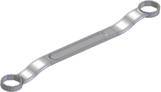
Ring Spanner
They can be placed on the nut only from the top and can be used with one hand without possibility of slippage.
Adjustable Spanners
As the name suggests the jaw size of the spanner is adjustable.
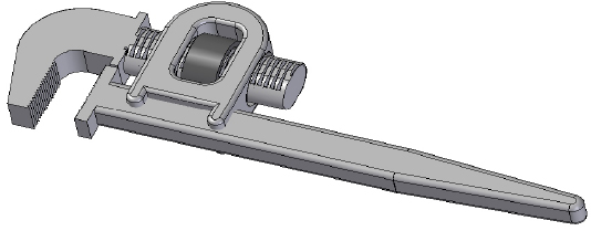
Adjustable Spanner
When no correctly fitting spanner is available, adjustable spanners are used.
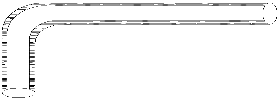
Allen Key
Allen Wrenches
Allen Wrenches are also known as Hexagonal Socket Bar Spanner (Allen Key). They are most useful for opening control knobs. These are right angled rods of hexagonal cross section with one short arm and one long arm.
Allen Wrenches
The short arm is used for assembly and the long arm is used for tightening. They also come as a set in metric or inch sizes. Allen Wrenches are most useful for opening many control knobs.
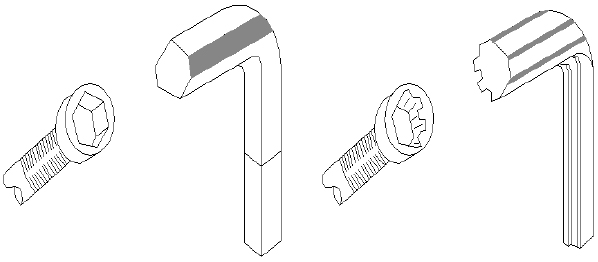
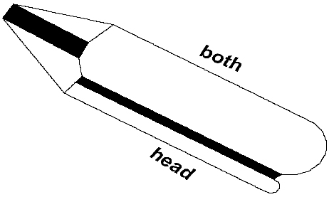
Screw Drivers
These are the most common tools for securing screws. Following are the two types of screw drivers:
Flat Blade Screw Driver
They are used in practice for slotted screws.
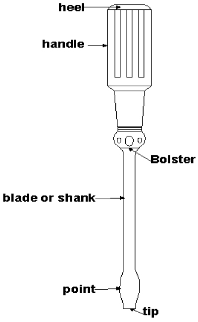
Standard Screw Driver
The above figure shows various parts of screw driver. The handle is usually made of tough, transparent colored plastic and shaped to provide a firm, comfortable grip. The handle has a smooth, semi-rounded heel which fits the palm comfortably.
The blade or shank is made of steel which is heat treated and tempered to apply torque to the screw head. The blade and tip are chrome plated.

Flat Blade Screw Driver
For a flat blade screw driver the width of the blade and the thickness of the blade should be correct.
Philips Head Screw Driver
These screw drivers have star-shaped holes in their heads as opposed to straight slots. There are four (No. 1 to No, 4) standard sizes of Philips screw drivers. No. 1 and No. 2 are usually needed.
Philips Head Screw Driver
The star-shaped hole in a Philip’s screw driver and the tip of a Philip’s screw driver must fit together properly so that the walls of the screw head or the tip of the driver, or both, will not be damaged.
In addition, there are some other special types of screw drivers which are used occasionally. For small and delicate work Jeweler’s screw driver sets are available. The barrel of the handle is knurled with a top finger rest.
Ratchet’s Screw Drivers have a selector level that will allow the screw driver to rotate freely in either the clockwise or anticlockwise direction and obtain the ratchet driving action in the other direction.
Nut Drivers
Nut drivers are used as screw drivers but are designed to accommodate hexagonal types of machine nuts instead of screw heads.
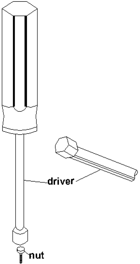
Nut Drivers
They are very useful in mounting a nut on a threaded stud and in holding a nut while its screw is being tightened.
Files
Files are made of hardened high carbon steel. Filing is the most important skill to be acquired in electronic fabrication. Files are classified according to their length, cut of teeth and cross-section. Following are files of different cross section:

Files of different cross section
During repair work, if there is a need to use a different sized replacement component, like a potentiometer or a fuse carrier. In those cases files are very useful to enlarge holes. They are also used to smooth the scratch marks on surfaces.
Practical Tips
- The technician should carefully see the size of the screw and the type of opening to select the particular driver.
- A screw driver should not be used at an angle to the screw.
- The technician should be cautious enough to insulate himself from electricity. The driver’s handle or covered blade is not enough for insulation.
- When filing soft materials, there is a possibility that the waste metal may clog the file teeth. In that case the file teeth should be cleaned using file cleaners.
- Never do filing near open electronic equipment as the filings may enter the equipment, causing electrical shorts.
3.2 Test and Measuring Instruments
There are many types of testing and measuring instruments available for electronic troubleshooting. A certain amount of personal opinion is involved in troubleshooting methods. One may prefer to use a voltmeter for troubleshooting problems, another may use oscilloscope leads. Although, a personal choice is always there, the technician should be familiar with all the methods, advantages and disadvantages, limitations, and types of troubleshooting instruments.
Analog and digital multimeter [volt-ohm-multimeter (VOMs)] is available for troubleshooting analog circuits.
Multimeter
The multimeter is the most useful instrument for the troubleshooting technicians. This instrument facilitates the measurement of DC voltage, AC voltage, DC current and resistance values. With proper accessories it can also measure other parameters like high frequency signals, high voltages and so on.
Voltmeters and ammeters both AC and DC and ohm-meters are available in various ranges and configurations. A multimeter is a combination of all these meters which makes it very useful in the field.
An analog multimeter is used when merely the presence of a value near one specified is required rather than a measured value that is exactly as expected. An analog indication of approximate voltage value is more quickly observed as compared to digital reading. They are less susceptible to extraneous noise.
When a high accuracy is required, especially when very small changes in a level need to be detected, a digital multimeter is preferred.

Analog Multimeter
Analog multimeter is the most widely used test and measuring instrument. It operates with a permanent magnet moving coil, which can become a DC voltmeter, an AC voltmeter, and DC milli-ammeter or an ohm meter. Sometimes an AC current measuring facility is also present.
It has a coil of fine wire wound on a rectangular aluminum frame. It is mounted in the air space between the poles of a permanent horse-shoe magnet. Refer to the following figure:

Moving coil meter
When electric current flows through the coil, a magnetic field is developed that interacts with the magnetic field of the permanent magnet to force the coil to rotate. The direction of rotation depends upon the direction of electron flow in the coil. The magnitude of the pointer deflection is proportional to the current. In usual meters, the full scale deflection (FSD) is about 90 degrees.
Using the Multimeter
The multimeter operates without any error if some preliminary adjustments are undertaken while using the multimeter. A scale plate of a standard multimeter is shown in the following figure:

Typical scale of Analog multimeter
Following are the settings of the multimeter:
- Place the multimeter flat on a bench with its face up.
- Set the range switch to OFF.
- Short two test probes together.
- Note if the meter pointer indicates exactly 0 at the extreme left end of the scale.
- If it does not read 0, turn the screw o the meter movement slowly until the proper 0 reading is obtained.
Measurement of Current
The moving coil meter is basically sensitive to current and is therefore an ammeter. For the direct current measurement, place the meter (ammeter to measure current) in series with the circuit. When the ammeter is included in the circuit, its internal resistance adds up, thereby reducing the current in the measuring branch. Usually, this resistance is small and can be ignored.
For alternating current measurement, rectifier type meters are used which will respond to the average value of the rectified alternating current. The meter has to be calibrated in amperes rms (root mean square) for the measurement of sine waves.
Measurement of Voltage
The current meter can be used to measure voltage. The moving coil meter has a constant resistance. So, the current through the meter is proportional to the voltage.
To measure the potential difference between two points, connect the two voltmeter leads to these points. So, in contrast with the ammeter, the voltmeter is connected in parallel with the circuit whose potential has to be measured.
To measure AC voltage, rectification is required. As in the AC current meters, AC voltmeters respond to the average value of the rectified voltage but are calibrated in volts rms for a sine wave.
Measurement of Resistance
The moving coil meter can be used to measure unknown resistance. Test probes are short circuited and the ohms adjust control is turned so that the current through the total circuit resistance has a full scale deflection.
An ohm meter is never used while the circuit is in operation. Sometimes the resistances depend upon the circuit conditions, in that case measure the voltage across the resistance, the current through it and calculate the resistance.
Operating Suggestions
- Set the range switch to the proper position before making any measurement.
- It is always advisable to start from the highest range in case of unknown measurement. Never apply more voltage or current than the amount noted in each position.
- Remove the parallax for the most accurate readings. Look at the scale from the point where the pointer and its reflection on the mirror come together.
- When the meter is not in use, keep the range selector in the OFF position and remove the batteries.
- Always connect the meter in series with the load when current is measured. Select the desired current range and connect the meter in series with the circuit under test.
- The polarity of the leads is not important when measuring AC. The sensitivity of the meter is different for the AC and DC ranges.
Practical Tips
- Do not measure voltage across a high-resistance or high impedance circuit with a meter that has relatively low input impedance.
- Do not use a meter to measure ICs with MOSFET unless you know the probes are static free.
- Avoid using a voltmeter (instead of a logic probe) to measure logic 1 and logic 0 in a digital circuit.
- In case of AC measurements, the meter movement responds to the average value of rectified current and therefore there could be an inaccuracy in measurement because of different wave shapes. If the applied waveform is non sinusoidal (square or triangular) then the rectified type of AC voltmeters is subject to errors. Therefore it is advisable to consult the manufacturer’s chart for the factors to be taken into consideration to get the correct value.
- The batteries in the meter should be checked frequently for correct operation in the resistance ranges.
Digital Multimeter
In the analog type of multimeter the value of the parameter being measured is estimated from the position of a pointer along a calibrated scale. Even when using a high grade meter of this type it is difficult to take readings with a precision which is better than about 1 percent of the full scale value.
This limitation is largely imposed by the physical arrangement of the scale and the pointer scheme. For more precise measurements it would be better if the actual value of the voltage or current could be displayed directly as a numerical value.
The digital meter displays the measurements as discrete numerical instead of a pointer deflection on scale. They have high input impedance and the user has to only set the function switch and read the measurement.
The basic function performed is an analog to digital conversion. The analog signal input might be a DC voltage, an AC voltage, a resistance or an AC or DC current. Thus a digital value is converted to a proportional time duration which in turn starts or stops an accurate oscillator. The oscillator output is fed to a counter which drives a digital readout arrangement in terms of voltage values.
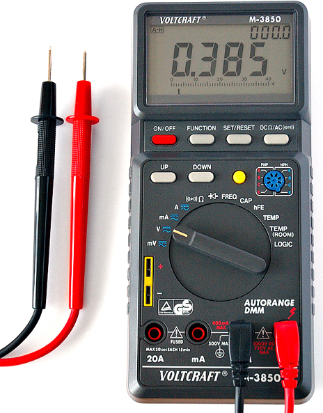
Digital Multimeter
DMM is classified according to the number of full digit displayed. An over range digit is an extra digit to allow the user to read values beyond full scale. An over range digit is sometimes known as ‘one half’ digit. For example if a signal changes from 9.999 to 10.012 a four digit display will require a change in range and the second measurement will read 10.01V. The 0.0002 will not be read. On a Four and Half digit display this problem will not occur.
Apart from reading the values of voltage, current and resistance, DMM can also be used to measure temperature, frequency, duty cycle, capacitance, and other parameters with the help of optional accessories. They are used to perform Diode Checks and Continuity Checks in a circuit.
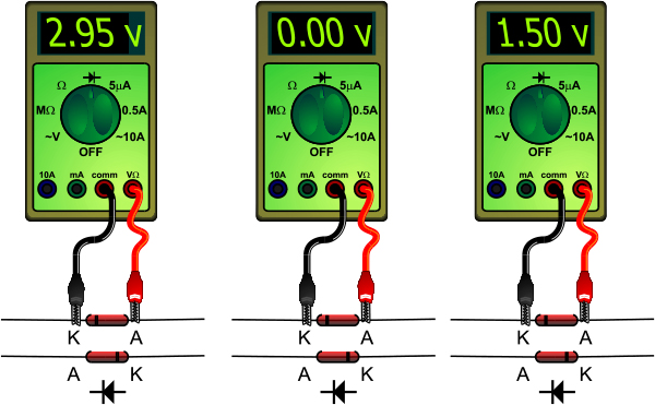
Diode Check using DMM
The diode is a semiconductor device, which conducts direct current in one direction only. In other words, the diode exhibits a very low resistance when it is forward-biased and an extremely high resistance, when it is reverse-biased. An ohmmeter applies a known voltage from an internal source (batteries) to the measured resistor. Theoretically, this voltage can reach 1.5 V or 3 V. The diode requires a voltage of 0.7 V to become forward-biased. Therefore, if the positive test lead of the ohmmeter is connected to the anode and the negative test lead of the ohmmeter is connected to the cathode, the diode becomes forward-biased. In this case, the ohmmeter reads a very low resistance. If the test leads are reversed with respect to the anode and the cathode, the diode becomes reverse-biased. Then, the ohmmeter reads a very high resistance. Thus an ordinary ohmmeter can be used to test a diode.
Most digital multimeters (DMMs) have a diode test function. It is marked on the select switch with a small diode symbol. When the DMM is set to diode test mode, it provides a sufficient internal voltage to test the diode in both directions. The positive test lead of the DMM (in red color) is connected to the anode, and the negative test lead of the DMM (in black color) is connected to the cathode. If the diode is in good working order, the multimeter should display a value in the range between 0.5 V and 0.9 V (typically 0.7 V). Then the test leads of the DMM are reversed with respect to the anode and the cathode. As the diode in this case appears as an open circuit to the multimeter, practically all of the internal DMM voltage will appear across the diode. The value on the display depends on the meter’s internal voltage source and it is typically in the range between 2.5 V and 3.5 V.
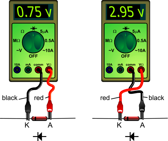
Properly Functioning Diode
A defective diode appears either as an open circuit or as a closed circuit in both directions. The first case is more common and it is mainly caused by internal damage of the pn-junction due to overheating. Such a diode exhibits a very high resistance when it is both forward-biased and reverse-biased. On the other hand, the multimeter reads 0 V in both directions if the diode is shorted. Sometimes a failed diode may not exhibit a complete short circuit (0 V) but may appear as a resistive diode, in which case the meter reads the same resistance in both directions (for example 1.5 V). This is illustrated in Figure 3.16.
Defective Diodes
As was mentioned earlier, if a special diode-test function is not provided in a particular multimeter, the diode still can be checked, by measuring its resistance in both directions. The selector switch is set to OHMs. When the diode is forward-biased, the meter reads from a few hundred to a few thousands ohms. The actual resistance of the diode normally does not exceed 100 Ω, but the internal voltage of many meters is relatively low in the OHMs range and it is not sufficient to forward-bias the pn junction of the diode completely. For this reason, the displayed value is higher. When the diode is reverse-biased, the meter usually displays some type of out-of-range indication, such as “OL”, because the resistance of the diode in this case is too high and cannot be measured from the meter.
The actual values of the measured resistances are unimportant. What is important, though, is to make sure that there is a great difference in the readings, when the diode is forward-biased and when it is reverse-biased. In fact, that is all you need to know. This indicates that the diode is working properly.
Oscilloscope
So far we have looked at meters which give a picture of the static levels of voltage or current. For more compete tests on the operation of a circuit, we need to be able to examine the way in which the signal varies with time. This involves displaying a graph of the signal being examined against a base of time, and the instrument employed for this is the Oscilloscope.
It gives a visual indication of what a circuit is doing and shows what is going wrong more quickly than any other instrument. Multimeter can detect the presence of signals and if the shape of the signal is known the average, peak, rms or peak to peak can be calculated. However, if the waveform is not known, then this is not possible. Noise may be superimposed on the signal and the multimeter will not be able to give the proper information. The oscilloscope gives a true and clear picture of the waveforms.
Understanding an Oscilloscope
The following figure shows all the essential controls on the front panel. The controls can be present in some different form than shown, but they have to be present in the oscilloscope.
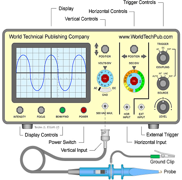
Controls on an oscilloscope
The controls are as follows:
- ON / OFF control
- Focus Control
- X and Y position controls
- Trigger, sync or Level control
- Intensity or Brilliance control
Sometimes the ON / OFF control can be combined with Intensity / Brilliance control.
The instrument is directly plugged in the mains supply. After switching on the instrument, wait for a while until the CRT heater warms up. Turn the Brilliance control to clockwise direction until you observe a horizontal line of the trace on the screen.
If the trace does not appear on the screen then turn the Brilliance control right up to the fully clockwise direction. Turn Time/cm control to the slowest speed, but not to the off position. With these settings, a light spot should appear on the screen moving slowly from left to right.
Still if nothing is seen, adjust the Trig/Level control in clockwise direction and observe if something appears. Adjust the vertical and horizontal position controls until the trace appears.
If all the above steps do not result in showing a trace on the screen, the instrument is faulty. Unplug the mains and check the fuses.
After getting a trace on the screen use vertical and horizontal position controls to start the trace at the left hand side of the screen and lie along the centre line. Focus control is used to get the line as thin as possible. Reduce the Brilliance setting to a comfortable viewing level.
When making oscilloscope measurements, a pair of probes is very valuable and this facilitates making a contact on the point of measurement in a convenient manner. Probes connect the measurement points in the device under test to the inputs of the oscilloscope.
Input Probes
When the signals being examined have relatively low frequencies, such as the waveforms expected of an audio amplifier, the capacitance of the test leads usually poses no problem and has little effect on either the waveform of the signal being displayed or the circuit being tested.
When high frequency signals or fast pulses are being examined the capacitance between the core and screen of the input cable can affect the waveforms that are displayed and may upset the circuit being tested.
The capacitance between the core and screen of a typical 1 meter long input cable could be about 50pF which, when added to 50pF input capacitance of the amplifier will give a total shunt capacitance of 100pF across the circuit being tested.
Suppose the circuit being examined is a video amplifier with a load impedance of 1K and the signal being examined is a 10Mz square wave. The displayed waveform on the oscillator will become triangular in shape because the capacitor is unable to charge and discharge fast enough through the amplifier load resistor to be able to follow the 10Mz square wave.
One way of overcoming this problem is a special probe at the input end of the test lead. This probe is usually arranged to act as a divide by ten attenuator and the circuit arrangement is as shown in the figure below:

Circuit arrangement of simple input probe
The dc component of the signal is attenuated by a pair of resistance, forming a simple potential divider. To balance up the capacitive reactance a small series capacitor is connected across R1. The value of this capacitor is adjusted so that it has a capacitive value which is 1/9 of that of shunt capacitance of the lead and the oscilloscope amplifier input.
For example where the oscilloscope has a shunt capacitance of the order of 50pF, the series connection capacitor becomes approximately 5pF. Now, when the probe is used to examine the video amplifier circuit, it presents an effective reactance of around 3K at 10Mz and will therefore have much less effect on the signal being examined.
Probe Tests
When a probe is included in the input line, it is important to match the probe to the oscilloscope input. This is usually achieved by adjusting the small compensation capacitor in the probe to produce the correct results on a square wave input. Most oscilloscopes provide a square wave test signal for setting up input probes. This signal is applied to the probe input and the probe capacitor is then adjusted to give a correct square on the screen.
If the compensation capacitor in the probe is too large, it will not produce the correct attenuation ratio for high frequency signals. In a square wave input this will give rise to overshoot on the edges of the square wave as shown in following figure:
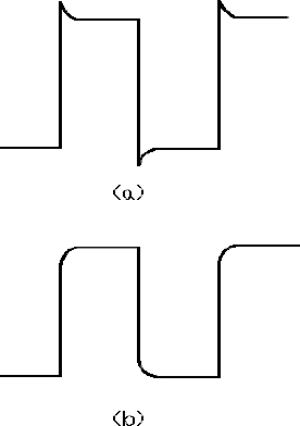
Effects of probe compensation adjustment (a), (b)
When the compensation capacitor is too small the higher frequencies are attenuated too much and this produces rounded corners on the square wave as shown in the figure (b).
With the correct setting of the compensation capacitor there could be no overshoot or rounding off on the edges of the square wave and the waveform is displayed correctly.
Calibration of the oscilloscope probe
When using an oscilloscope, it is very easy to plug the oscilloscope probe in and start to make measurements. Unfortunately oscilloscope probes need to be calibrated before they are sued to ensure that their response is flat. There is a built in calibrator on virtually every oscilloscope for this purpose. It provides a square wave output, and there is a small preset adjustor on the probe. With the oscilloscope probe connected to the output of the calibrator the shape of the waveform displayed on the screen should be adjusted until it is perfectly square. If the high frequency response of the probe is down then the edges of the square wave will be rounded. If it is up then the square wave edges will show overshoot.
Although a simple adjustment, it is essential that it is undertaken to ensure that the performance of the probe is correct.
Measuring Amplitude with Oscilloscope
Oscilloscope’s greatly and effectively help in finding out the amplitude of voltage.

Voltage measurement
The number of centimeters on the vertical scale from the negative peak to the positive peak is counted. This count is multiplied by the setting of the volts per centimeter switch.
For example: if 5 V/cm is the volts/cm setting and the waveform measures 4.8V from peak to peak then the waveform voltage is 4.8 * 5 = 24V Peak to Peak.
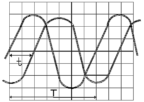
Measuring Frequency with Oscilloscope
For frequency measurement the time period of one complete cycle is measured. This is merely the horizontal distance between the two identical points on the neighboring waves.

Frequency measurement
This distance is then multiplied by the setting of the Time/cm switch and the period of one cycle is calculated. The reciprocal of this time is the frequency of the wave.
For example if the peaks of the waveform are 5 cm apart, and the Time / cm switch is set to 200 μ s / cm, the time of one complete cycle is 5* 200 = 1000 μ s = 1 ms and the frequency is 1 / 1000 = 1 KHz.
Measuring Phase Difference
If we have two signals of the same frequency and wish to measure the phase difference between them, we can do it by using a dual trace oscilloscope. One signal is fed to CHANNEL1 input and the other to CHANNEL2 input.
The VH1 position is adjusted to place the CH1 Trace so that it is centered about the horizontal axis of the screen. The CH2 trace is then moved to place it over the CH1 trace. The X position control is then adjusted to move the point where the CH1 trace crosses horizontal axis to line up with the left hand vertical line.
The distance between the crossing point of the CH1 trace and the corresponding point of CH2 trace is then measured along the horizontal axis as shown in the following figure. The total period of one cycle of CH1 waveform is also measured:
Measurement of Phase difference
The phase shift will be the difference in position between the two traces divided by the total wave period and the result is multiplied by 360 to get phase in degrees.
Lissajous Figures
If we have to compare the phase relationship between two AC signals, then apply one signal to X plate of the tube and the other signal to Y plate of the tube. This produces a display which is generally referred to as Lissajous figure.
On dual trace oscilloscope there is usually a position of TIME / DIV switch which selects the CH2 signal. With this mode selected one signal is applied to the CH1 input and the other to the CH2 input.
When the two signals applied have the same frequency and are exactly in phase, the result will be a diagonal line on the cathode ray tube which will run from the bottom left of the screen to the top right as shown in the following figure(a):

Typical Lissajous figures display
If one of the signals is now reversed in polarity, so that it is 180 degrees out of phase with another signal, the result is still a straight diagonal line but now it will run from the top left to bottom right of the screen as shown in figure (b).
When two signals are not quite in phase with one another, the diagonal line changes to an ellipse running diagonally from bottom left to top right of the screen as shown in figure (c).
As the phase difference is increased, the thickness of the ellipse will increase until it becomes a circle when the signals are 90 degrees out of phase as shown in figure (d).
The above results assume that the signals being compared are sine waves which are of the same amplitude. It is also assumed that the deflection sensitivities of X and Y circuits of the oscilloscope are the same. If the signal amplitudes or deflection sensitivities are not identical then the resultant image will be stretched in a direction with higher sensitivity.
When the waveforms being examined are not sine waves the Lissajous display becomes distorted but generally follows a similar type of pattern.
Analyzing waveform with Oscilloscope
An oscilloscope is an excellent tool to see what is happening in the circuit and with experience much can be gained from the correct interpretation of what is displayed.
If a sine wave is given to an amplifier and the oscilloscope displays a flat topped waveform when connected at its output, it means that clipping is taking place in the amplifier.
Calibration of Oscilloscopes
Oscilloscopes have always been an important measurement tool for the engineer. The design of oscilloscopes has evolved slowly from early instruments which were used to simply view a waveform, to oscilloscopes with calibrated ranges and graticules (grid) on the display to enable measurements to be made, up to the modern digital storage oscilloscope (DSO) which have many advanced measurement functions built in as standard. The latest designs now use digital LCD displays instead of the tradition CRT (cathode ray tube) and are putting even more measurement power in the hands of the engineer in ever more portable instruments. The oscilloscope is still evolving, the latest step is the scope meter which combines the functions of an oscilloscope with those of the DMM in one instrument. Each evolutionary step has added to the measurement capability of the oscilloscope, making the calibration of these instruments even more important.
All types of oscilloscopes require calibration of these main functions.
Oscilloscope Calibration : Amplitude
The oscilloscope amplitude is calibrated by applying a low frequency square wave and adjusting its gain to meet the height specified for different voltage levels (shown by the graticule line divisions on the oscilloscope). The voltages that are used for calibration are selected using the corresponding setting as per the amplitude ranges on the oscilloscope. Using this output the waveforms should be aligned with the graticule markings on the oscilloscope display. When calibrating the oscilloscope’s amplitude gain, it isl needed to set different voltages and check that the gain matches the graticule height lines on the display of the oscilloscope within the specifications as supplied by the oscilloscope’s manufacturer.
Oscilloscope Calibration : Time base/horizontal deflection
The time base of an oscilloscope is calibrated to ensure the horizontal deflection meets the manufacturers specifications. A time marker signal is generated from the calibrator of which the peaks are aligned with the graticule scale on the oscilloscope display.
Oscilloscope Calibration : Bandwidth reference
Calibration of bandwidth requires a constant amplitude sine wave of variable frequency up to and above that of the oscilloscopes specification. Many calibration procedures also call for a 50kHz reference level to set the start amplitude.
Oscilloscope Calibration : Trigger level
Trigger level can be tested by using a sinusoidal signal at 6 divisions high and adjusting the trigger level control to produce a stable trace starting at any point on either the positive or negative slope depending on scope selection. Sensitivity is tested by applying a much smaller signal (typically 10% of FS) and checking a stable trace can be obtained even when the position controls are used to move the trace to the top or bottom of the display. Bandwidth of the triggering and operation of the HF noise filters on some scopes can be tested by using the leveled sweep output and increasing the frequency or until stable triggering is lost.
Precautions
Make the following settings before switching on the oscilloscope or after completion of its use:
- Tune the stability control to auto
- Turn the intensity control to a fully anti-clockwise position
- Set vertical and horizontal position controls to midway round
- Turn volts / cm control to highest value of its range
- Set Time / cm control to 1 ms / cm or its nearest value
Use fully screened probes at high frequencies to avoid possibility of signal degradation. The use of a compensated probe unit reduces the effect due to amplitude attenuation and phase distortion in a coaxial cable.
Keep the beam intensity down to the minimum required for a particular setting.
Make sure that the vertical gain control is set above the voltage of the signal to be measured. Start with the highest voltage setting and minimum sensitivity, then work down the range until the correct setting is reached.
Avoid displaying a stationary bright dot for a long time. It may burn the phosphor on the screen.
Continuity Testers
The simplest form of resistance measurement is a continuity test which merely checks to see if there is a conducting path between two points in a circuit. This test simply indicates whether the resistance between two points is high or low and is convenient for tracing individual wires through a multi-wire cable or for tracing out track connections on a printed circuit board. One popular circuit for a continuity tester is shown in the following figure:
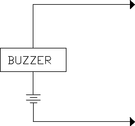
Continuity tester using a buzzer
Here a buzzer is connected in series with a battery and the two test leads. One test probe is connected to one end of the wire or circuit that is to be checked and the second probe is applied to the other end of the circuit. If the resistance between the two test points is low, the buzzer sounds to indicate continuity.
As an alternative to the buzzer the continuity tester might use a filament lamp or a light emitting diode as continuity indicator as shown in the following figures. The lamp or LED lights up when continuity is detected between the points to which the test probes are applied:

Continuity tester using (a) filament (b) LED
Waveform Generators
Most modern audio signal sources provide not only a sine wave but also square and triangular wave signals as well. These instruments are generally referred to as waveform generators to distinguish them from ordinary signal generators which produce only a sine wave output.
In this instrument the basic triangular waveform is generated by using a capacitor charged and discharged at constant current as the timing device. The basic block diagram of such a device is shown below:

Block diagram of waveform generator
The triangular signal is generated by using the voltage produced across a capacitor which is charged and discharged alternately by being switched to current source I1 and sink I2. The voltage the capacitor is fed to a pair of level comparators which detect when the capacitor voltage reaches two preset voltage levels. The output of the comparators drive a flip-flop which in turn switches the constant current sources I1 and I2 via switch S1.
For the rising slope of the triangular wave the capacitor is switched so that it charges linearly with time from current source I1. When the capacitor voltage reaches the reference level of comparator A1, the output of A1 triggers the flip-flop circuit and this in turn operates switch S1. The capacitor is now discharged by the current source I2 and falls linearly with time until it reaches the reference level of comparator A2.
The output of A2 is used to reset the flip-flop and this operates switch S1 so that the capacitor again discharges from I1 to start the new oscillation cycle. The result is that the voltage across the capacitor rises and falls linearly between the two reference levels to produce the triangular output waveform.
The amplitude of the waveform is determined by the voltage reference levels applied to the two comparators and the frequency by the value of the capacitor and the levels of current from generators I1 and I2.
Since the flip-flop switches state each time the triangular reverses its direction, the output from the flip-flop is a square wave whose frequency is the same as that of triangular wave.
The square wave produced will be 90 degrees out of phase with the triangular wave since the flip-flop is switched at the peaks and troughs of the triangular wave.
Resistance Boxes
For experimental troubleshooting, a switched resistance box is a useful accessory. The ideal arrangement is a true decade resistance box giving perhaps three decades of selectable resistance. The basic circuit arrangement of this type of resistance box is shown in the following figure:
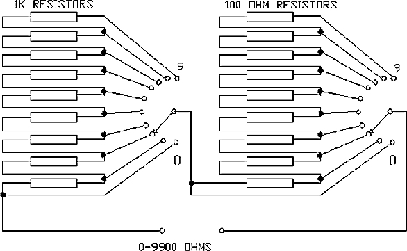
Arrangement of a decade resistance box
For simplicity the diagram shows only two decades. In this arrangement the box provides a range of resistance from 0 to 9.9KΩ in 100Ω steps. A typical box might have four banks with the lowest, giving 10Ω steps and the highest giving 10KΩ steps which would allow resistance values from 0 to 99.99KΩ to be selected in 10Ω steps.
Thus in a 10kΩ bank each resistor has the value 10kΩ. At the zero position the bank is shorted out but as the switch rotor is moved 10k, resistors are added in series between the rotor and the input terminal.
The output of a 10k bank switch feeds the top end of the 1k resistor bank and here the switch adds a selected number of 1k resistors in series. The 100Ω and 10Ω banks are wired in the same way and finally the wiper of the 10Ω selector switch comes out to the other input terminal of the resistance box.
The switches can be decimal type thumbwheel switches and the resistors in this type of box need to be at least 1 percent tolerance metal oxide types to give useful results.
For a home constructed unit using 1 percent components only the two most significant digits of the reading on the selector switches should be considered valid when assessing the value of resistance. In a commercial resistance box, the resistors are usually 1 percent tolerance components which have been measured and selected to give the correct values to within 0.1 percent or better.
Capacitor Boxes
It is possible to have a switched capacitor box which operates in a similar way to the resistor box. In this case the capacitors in each decade are connected successively in parallel to produce the desired value of the capacitor and the total capacitance of each decade is connected in parallel with that of the other decades.
Because of stray capacitance effects, about the lowest increment of capacitance that is practical would be 100pF. Thus a box could be built with the first decade going up to 1nF and successive decades to 10nF, 100nF and 1µF respectively.
For the lower decades polystyrene or silver mica capacitors with 2 percent tolerance might be used to give reasonable accuracy and good stability. For the higher ranges metallised polyester film capacitors of 5 percent tolerance might be used.
3.3 Safety Issues – Test and Tagging of Portable Electrical Equipment
Testing and tagging is the process of visually inspecting and electrically testing in-service electrical equipment.
The aim of test and tagging is to determine if the appliance is electrically safe for personal use. The appliance undergoes a visual inspection for defects such as damage or missing components and a number of electrical tests to measure earth continuity, insulation resistance and polarity.
Test and Tagging is sometimes referred to as PAT Testing (UK). This terminology was first used in the United Kingdom. A Portable Appliance Test or PAT, is a process by which electrical appliances are routinely checked to see whether they are safe. The term PAT – PAT Testing – more accurately describes the actual test equipment used by technicians (not the appliance being tested) as it is generally hand held and/or portable.
In Australia and New Zealand, this is done using the Standard; AS/NZS 3760:2010 “In-service inspection and testing of electrical equipment” as a reference document.
PAT tests include:
-earth resistance test
-earth continuity test
-insulation resistance tests
-polarity checks etc.
In addition to above the regulations require that wherever any plug, socket or adapter is supplied, that it complies with the appropriate current standard. This means that they must conform to the relevant British Standards (i.e. BS1363) or approved alternatives. British Standard BS1363 covers 13 Amp fused plugs, switched and unswitched sockets. The standard now requires that the live and neutral pins on plugs are part insulated so as to prevent shocks when removing plugs from sockets.
3.4 Summary
The multimeter facilitates the measurement of DC voltage, AC voltage, DC current and resistance values.
The analog multimeter can become a DC voltmeter, an AC voltmeter, and DC milli-ammeter or an ohm meter. The digital meter displays the measurements as discrete numerical instead of a pointer deflection on scale.
An oscilloscope gives a visual indication of what a circuit is doing and shows what is going wrong more quickly than any other instrument. Amplitude and frequency can be measured with an oscilloscope.
The Continuity tester checks to see if there is a conducting path between two points in a circuit. In a Waveform Generator, the basic triangular waveform is generated by using a capacitor charged and discharged at constant current as the timing device.
In the last chapter we have seen various tools, testing and measuring instruments. In this chapter we are going to study troubleshooting of passive and active components. The chapter also emphasizes testing of some other active components such as JFET, MOSFET, UJT, SCR, DIAC, TRIAC, LED, Photo detectors, Op-amp and Timer IC555. The equipment required for testing are Digital Multimeter / Analog Multimeter, Scientific Oscilloscope and test jigs.
Learning objectives
- Study testing of Active and Passive components
- Understand testing of JFET
- Study the testing of MOSFET
- Know what are the safety precautions to be taken while testing MOSFET
- Study testing of UJT, SCR, DIAC, TRIAC
- Understand how to test LED, photo detectors, Op-amp, Timer IC
- Test the semiconductor devices using oscilloscope
4.1 Testing of Passive Components
Passive components include resistors, capacitors and inductors. Passive components can not amplify or oscillate a signal. Let us now go through the testing procedure of these one by one.
Testing of Resistors
Resistance is the opposition to the flow of current offered by a conductor, device or circuit. According to Ohm’s Law:
R = V / I in ohm, Where:
R is Resistance (ohm)
V is Voltage (volts)
I is Current (amperes)
Basically resistors are categorized into two types:
Fixed Resistors
They come in following forms:
- Carbon Composition Resistors
- Metal Film Resistors
- Wire Wound Resistors
Variable Resistors or Potentiometers
They can be divided into three categories depending upon resistive material used:
- Carbon
- Cermets
- Wire wound
Depending upon the number of resistance and control arrangement they are divided into:
- Single Potentiometers
- Tandem Potentiometers
- Twin Potentiometers
- Multi-turn Potentiometers
Testing of Fixed Resistors
- The normal range of resistors encountered in practice is 1 ohm to 10 mega-ohms. The most convenient method of checking the resistance is by using an ANALOG or DIGITAL MULTIMETER.
- Digital multimeter can be used to measure very low resistance values such as the contact resistance of plug and socket connectors, etc.
- The following steps are performed to check the resistance value:
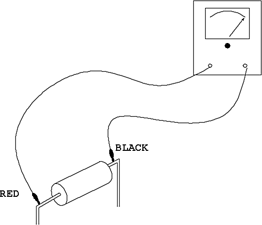
Testing method for fixed resistor
Procedure
- Fix the given resistor on the bread board.
- Set the multimeter in the ohm-meter range and connect the ohm-meter leads across the resistor.
- Check the value shown with the value indicated by the color code on the resistor.
- Open or short of the resistor is shown by infinite or zero resistance in the meter.
- The total measurable resistance range in the VOM is divided into three ranges:R * 1 0 to 2K ohms
R * 100 to 200 K ohms
R * 1000 t0 20 M ohms - Before the unknown resistor is tested, the two meter leads are shorted together and the zero control corresponding to the range selected is adjusted to read zero ohms on the scale. With the unknown resistor connected for test, the current falls, and the scale is non-linear.
Testing of Variable Resistors or Potentiometers
- Variable resistors basically consist of a track of a resistance material to which a movable wiper makes contact.
- They are typically used to set bias values of transistors, setting time constants of RC timers, making gain adjustments of amplifiers, etc.
- Potentiometers can be checked in a similar way as that of fixed resistors using an OHMMETER. Following are the steps:

Testing of Potentiometer
Procedure:
- Connect either set of contacts (A or B) to the potentiometer as shown in the figure.
- Set the multimeter in the ohm-meter range and connect the ohm-meter leads as shown.
- The value is shown in the ohm-meter as per the central contact is wiping the resistor.
- As the shaft of the pot is turned, the resistance will be observed. If the resistance remains at zero or stays at an infinite reading, the pot may be replaced.
Testing of Capacitors
- A capacitor (or condenser) consists of two conductors separated by a dielectric or insulator. The dielectric can be paper, mica ceramic, plastic film or foil.
- It is measured in farads and the usual sub-units used are microfarad and Pico farad. Generally, the value of the capacitor is indicated on the body of the capacitor either in words, numbers or in the form of the color code.
- The polarized capacitors (1 microfarad and above) are tested using ANALOG MULTIMETER and DIGITAL MULTIMETER. Following are the steps involved:
Procedure
- Fix the given capacitor on the bread-board.
- Set the meter in the highest ohms range.
- Connect the ohm-meter leads across the capacitor.
- In case the capacitor is good, the meter pointer moves quickly towards the low-resistance side of the sale and slowly recedes towards infinity.
- Open or short of the capacitor is shown by infinite or zero resistance in the meter.
- If the capacitor is leaky, the final value of the resistance indicated by the ohm-meter will not be very high (below a few kilo-ohms).
- Digital multimeter tests the value of the capacitor from a few Pico farads to 20 microfarad. An open capacitor will show zero and a short capacitor will show overload on this range.
- DMM just measures capacitance and does not test for leakage, ESR (Equivalent Series Resistance) or breakdown voltage.
- For small capacitors (0.01 microfarad or less), just a momentary deflection is seen on the Analog multimeter when the probes are touched to a capacitor. A DMM may not provide any indication at all.
- Capacitance meters are available for measuring the value of capacitance and are more accurate than DMM for this purpose. They measure the value of capacitance ranging from 1 Pico farad to 1000 microfarad. Similarly, ESR testers measure the Equivalent Series Resistance.
Tips
- Any capacitor that measures a few ohms or less is bad. Most should show infinite resistance value even on highest resistance range.
- The best way to really test a capacitor is to substitute a known good one. A VOM or DMM will not test the capacitor under normal operating conditions or at its full-rated voltage. So substitution is the quick way of finding a faulty capacitor and solving major fault problems.
Testing of Inductors
- Inductance is the characteristic of a device which resists change in the current through the device.
- The unit of inductance is Henry. The value of inductor may be printed on the component body or it may be printed with color bands. The primary use of inductors is filtering (power supply filtering and signal filtering). They can be tested by using Analog or Digital Multimeter. Following are the steps involved:
Procedure
- Fix the given inductor on the bread board.
- Set the ohm-meter in lowest ohm range.
- Connect the ohm meter leads across the inductor.
- An open inductor shows infinite resistance in the ohm meter.
Note
- Keep your fingers away from the conductor because body resistance lowers the reading.
- Values of Capacitor and Inductor cannot be checked with Ohm meter.
Testing of Resistor, Capacitor and Inductor Using Oscilloscope
- This can be done on a oscilloscope which has a component test facility. This facility is used for instant display of a test pattern to indicate whether or not the component is faulty. The oscilloscopes are requires to have a built-in Component Tester (CT).
- The indicating range of the CT is limited to a range of 20 ohms to 4.7 K ohms. Below and above these values, the test pattern shows only short circuit or open circuit.
Using the Component Tester
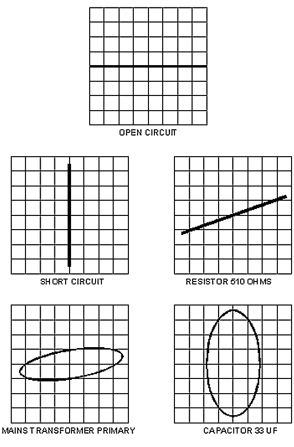
Test Pattern for single component
The CT is switched on by depressing the CT push-button. A shortened horizontal trace will be observed. For the component connection, two simple test leads with 4 mm banana plugs are required. The test leads are connected to the insulated CT socket and the adjustment ground socket in Y-section.
Procedure
- Set the scope in component testing mode.
- Connect the leads across resistor/capacitor/inductor.
- Observe the test patterns displayed by the resistor/capacitor/inductor under test.
- Open circuit is indicated by straight horizontal line.
- Short circuit is shown by a straight vertical line.
- A horizontal ellipse indicates high impedance or a relatively small capacitance, or a relatively high inductance.
- A vertical ellipse indicates small impedance or a relatively large capacitance, or a relatively high inductance.
- A sloping ellipse means that the component has a considerable ohmic resistance in addition to its reactance.
Precaution
- Do not test any component in a live circuit. Remove all grounds, power and signals connected to the component under test.
- During an in-circuit test make sure the circuit is dead. No power from mains/line or battery and no signal inputs are permitted. Remove all ground connections inclusive of safety earth (pull out power plug from outlet). Remove all measuring cables including probes between oscilloscope and circuit under test.
4.2 Testing of Semiconductor Devices
Semiconductor Devices
Semiconductor diodes are broadly classified into two areas:
Bipolar: where the device action depends upon the flow of the type of charge carriers across forward or reverse biased p-n junction. In an n-p-n transistor, the current is controlled by a forward biased base-emitter junction. The commonly used bipolar devices are transistors, diodes, UJT, Thyristor, Logic ICs (TTL) and Linear ICs.
Unipolar: where the devices use only majority carriers for current flow which is controlled by an electrostatic field. FET, MOSFET, CMOS logic and some linear ICs are some good examples of unipolar devices.
Diode Testing
Please refer Chapter 3 for diode testing using DMM.
Testing Zener Diode
- A zener diode has a very high resistance at bias potentials below zener voltage. This resistance could be worth several mega ohms. At zener voltage, the zener diode suddenly shows a very low resistance, say between 5 and 100 ohms.
- An ohm meter can detect a short or open zener diode in the same way as with a regular diode. However, this test does not determine if the diode will operate properly at its specified zener voltage.
- A simple test can be performed using a power supply that has a higher voltage than breakdown voltage Vz of the diode:
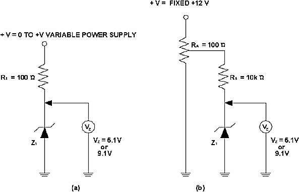
Testing of zener diode
- The power supply can be variable or fixed. The power supply voltage is gradually increased. The voltage across the diode will follow the increasing voltage until it reaches the breakdown point (Vz), beyond which an increase in power supply voltage will have little effect on the Vz point of diode.
- A DMM on its diode test range may read the actual zener voltage if it is very low but will read open otherwise.
- The most common failure will be for the device to short read 0.0 ohms in both directions. Then, it is definitely dead.
Testing Tunnel Diode
- A tunnel diode (TD) is a p-n junction which exhibits a negative resistance interval. Negative resistance values range from 1 to 200 ohms for various types of tunnel diodes.
- They are utilized in switching circuits. A TD is evaluated using a saw tooth output waveform from an oscilloscope as a current source:
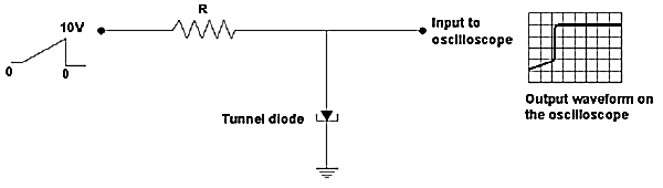
Testing of Tunnel diode
- A 670ohm resistor from the saw tooth out connector in series with TD to ground will give a calibrated current/div horizontally (say 1 mA/div).
- The saw tooth voltage goes from 0 to 10 volts. Therefore, the horizontal display becomes current/div. Looking at the voltage drop across the diode will give a vertical display of the low/high voltage state of the diode.
- The display does not give an indication of switching time but confirms that the device has the ability to switch at the correct current level and will probably perform normally in the circuit.
4.3 Testing Bipolar Transistors
About Transistors
- Transistor is the most commonly used semiconductor device in electronic circuits. In troubleshooting transistor circuits the following points should be kept in mind.
- The n-p-n and p-n-p devices are basically ‘off’ devices while vacuum tubes are basically ‘on’ devices.
- In normal operation, base-emitter diode is forward biased and base-collector diode is reverse biased.
- Shorting base to emitter turns off transistor, while forward biasing base-emitter junction turns on transistor. Shorting collector to emitter simulates saturation, as the transistor behaves like a closed switch.
- All transistors have a leakage current across their reverse biased base collector diode.
- Leakage current may be measured by shorting the base-emitter junction and measuring the voltage across the load resistance.
- Leakage current increases with temperature and doubles about every 10 degrees Celsius.
Testing Bipolar Transistors
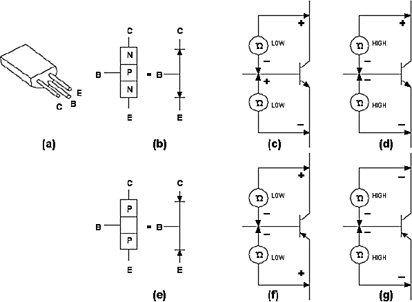
Testing bipolar transistor with an ohm meter
- For ohm meter testing purposes, an NPN transistor is similar to two diodes back to back as shown in figure (b).
- The two PN junctions, base-emitter and base-collector, when forward biased by the ohm meter, with positive lead to P terminal and negative lead to N terminal, should show a low resistance indication. Refer figure (c).
- There should be a high resistance reading when these junctions are reversed biased, positive lead to N terminal and negative lead to P terminal. Refer figure (d).
- The PNP transistor can be tested in a similar method, except that the diodes are face to face as shown in figure (e).
- This simple test determines if the transistor is shorted or open.
- After all, a good check of transistor operation is its actual performance under operating conditions. A transistor can most effectively be checked by substituting a new piece for it or one which has been checked previously.
Transistor hfe Testers
- Although an ohm meter can identify connections and show up transistors which are total failures, a more useful check on the function of a transistor is to measure its hfe characteristics under dc operating conditions.
- The parameter hfe is a measure of the ratio of the change in collector current to change in base current when the transistor is connected in common emitter configuration. A simple test rig for testing hfe is shown in the following figure:

Test rig for measurement of hfe of n-p-n transistor
- The switch S2 should first be set according to the type of transistor being tested, since n-p-n and p-n-p types are designed to operate from opposite polarity supply voltages. In case of an unmarked transistor a simple test with an ohm meter can determine the type.
- With switch S1 open, the collector emitter leakage current Iceo can be checked. For a silicon transistor this will usually be zero, but for a germanium transistor some current will flow depending upon ambient temperature.
- When S1 is closed, a current of 10micro Amp is fed into the base and this will cause the collector current to flow. The collector current will be approximately equal to the base current multiplied by the hfe of the transistor.
- Typical general purpose transistors might be expected to have an hfe of 50 to 500. If the meter is rated at 5mA, then the value of hfe can be read off the meter scale with a full scale deflection indicating an hfe of 500.
4.4 Testing Other Active Components
The field effect transistor is a voltage operated device. Unlike a bipolar transistor, a FET requires virtually no input (signal or bias) current. This gives it an extremely high input resistance, which is its most important advantage over a bipolar transistor. There are two major categories of FET: junction FET and MOSFET (metal oxide semiconductor FET). These are further sub-divided into p-channel and n-channel.
With zero gate-to-source bias, these devices are off, and are increasingly turned on by the application of increasing gate-to-source bias. This bias is positive for n-channel type and negative for p-channel type.
FET has three terminals named source, drain and gate (which correspond to emitter, collector and base of junction transistor). Source and drain leads are attached to the same block (channel of n or p semiconductor material). A band of oppositely doped material around the channel between the source and drain leads is connected to gate lead.
Failures in Field Effect Transistors
- In case of insulated gate FET, the insulation is between gate and channel. In fact this insulation is nothing but a delicate capacitor. The insulation is so thin and the gate is so small that it can be easily ruined:

Failures in Field Effect Transistors
- It is necessary to watch out for the static charge from fluorescent lights if the gate is left open. This can happen before the FET is installed, if after removing from its insulated case, is left on a table with its shorting wire removed. A shorting wire is usually a small piece of wire wrapped around all the leads.
Testing JFET
- For testing JFET, if you do not know the connections, then first find the two connections in which a small current will pass in either direction. The connections are the source and drain connections. In the third electrode, the gate, the current should pass only in one direction to either of the two electrodes.
- Keeping the gate positive, if the conduction takes place, the device is n-channel, whereas, if the conduction takes place when the gate is negative, the device is of p-channel polarity:
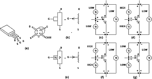
Testing JFET with an ohm meter
- The N-channel JFET is similar to a diode with its cathode connected to the middle of the resistor. Refer to Figure (a). The terminals D, G and S correspond to Drain, Gate and Source respectively.
- Figure (b) shows n-channel JFET, where the arrowhead points from p-type gate to n-type channel. The ohmic resistance from source to drain is also shown. Figure (e) shows p-channel JFET. In this type, the current direction and voltage polarities are reversed.
- The ohmic resistance of the channel should be about the same regardless of the polarity of the ohm meter lead connections from source to drain. It is the dc resistance of the channel when the depletion regions are absent, for example when the device is biased on in the channel ohmic region of characteristics. It is typically 100 Ω or much less.
- Refer to figures (b), (c), (f) and (g) for the connections for testing. There should be low resistance reading, with the positive lead on the gate and negative lead on the source or drain. The reading should be infinite when the negative lead is on the gate and the positive lead is placed on the source or drain.
- The same procedure is used for P-channel JFET, except that the diode’s anode is connected to resistor and the ohm meter polarities are reversed.
Testing MOSFET
- It corresponds to metal oxide semiconductor FET. There can be two types of MOSFET: Enhancement type or depletion type. Most MOSFET transistors are of Enhancement Mode type devices.
- The usual failure mode in a MOSFET is short between the gate and source, and the drain and source, i.e. everything is connected together:

MOSFET Test Circuit
- A method of testing FET, whether JFET’s or MOSFET, involves checking to see if the appropriate voltage on the gate causes the devices to conduct current from source to drain.
- A simple ohm meter check may not be used with MOSFET, although a check of PN junction from gate to source or drain will give some indication of correct operation in a JFET.
- A go/no-go test that is appropriate for N-channel depletion types (JFETs or MOSFET) and P-channel enhancement type (MOSFET) is shown in Figure 4.10.
- For an N-channel depletion type, when the switch is open sufficient drain current should flow through the 270 ohm resistor to forward bias the bipolar transistor, and the LED should glow.
- If the switch is now closed, the FET should be biased off, and the light should go off. If the LED lights no matter which position the switch is, the FET is shorted. If the LED does not light in either position of the switch, the FET is open.
- For a P-channel enhancement type, the reverse indications of the LED would be observed. By changing the polarity of the gate supply, other transistor types (P-channel depletion, N-channel MOSFET) may be tested.
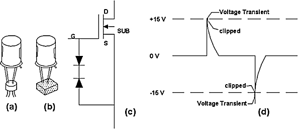
MOSFET safety precautions
- As compared to other semiconductor devices, special care must be taken for MOSFET. The SiO2 layer is so thin, that if a static charge of even less than 100V is applied across the gate and channel, the oxide layer may rupture. This usually results in gate leakage current, which renders the MOSFET useless.
- Static charges may occur on the leads of a MOSFET by rubbing on plastic bags or fabrics during shipping. Manufacturers ship MOSFET with their leads shorted together by means of a shorting ring, wire or foil and they are pressed into a conducting foam material, as shown in the above Figure 4.11 (a) and (b). The shorting devices should not be removed until MOSFET is installed on the circuit.
- The following precautions should be taken while handling MOSFET:
- Turn off the power to the circuit being worked on. Voltage transients developed by separating components or operating circuits may damage the MOSFET.
- Use a special ‘grounding wristband’ or connect a clip lead from your metal watchband to the chassis or ground point of the circuit.
- The user should ensure that his body and hands are at ground potential.
- The soldering iron should be properly grounded or clip lead connected from the tip of the tool to the chassis. Soldering guns are not recommended for use on MOSFET.
- Few newer types of MOSFET have zener diode protection from the gate to source, as shown in figures (c) and (d).
- Typically these diodes will breakdown and conduct when the voltage between gate and source exceeds 15 V, thereby protecting MOSFET from in-circuit transient voltages and out-of-circuit handling operations.
Testing UJT
- The unijunction transistor is also known as double base diode. It consists of a small p-type emitter connected to a bar of n-type material. Figure 4.12 uses a circuit symbol in which the arrowhead points in the conventional current direction for a forward bias junction. In this case it points from p-type emitter to n-type bar:
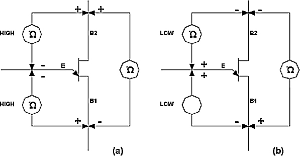
Testing a UJT with ohmmeter
- The PN junction of a UJT can be tested with an ohm meter similar to testing diodes and bipolar transistors. With the negative lead placed on the emitter and the positive placed at either base B1 or B2, the junction is reverse biased and the resistance should be high or infinite.
- When the positive lead is placed on an emitter and the negative lead is placed on either B1 or B2, the junction is forward biased and the resistance should be low.
- There could be a resistance reading of several thousand ohms when the meter is placed across the base leads.
Thyristors
- Thyristors are used extensively in power control circuits. The thyrister is basically a four layer p-n-p-n device and can be represented as a two-transistor combination structure. The two transistors out of which one is NPN and the other is PNP are cross connected.
- The base of NPN is connected to the collector of PNP and the base of PNP is connected to the collector of NPN. The following figure (a) shows the device structure and symbol of SCR and figure (b) shows different forms of SCR packages.
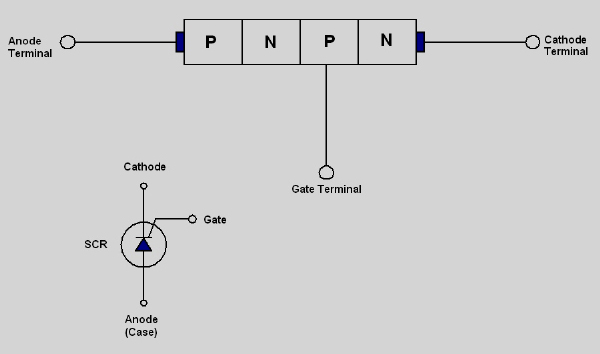
SCR (a)—device structure and symbol
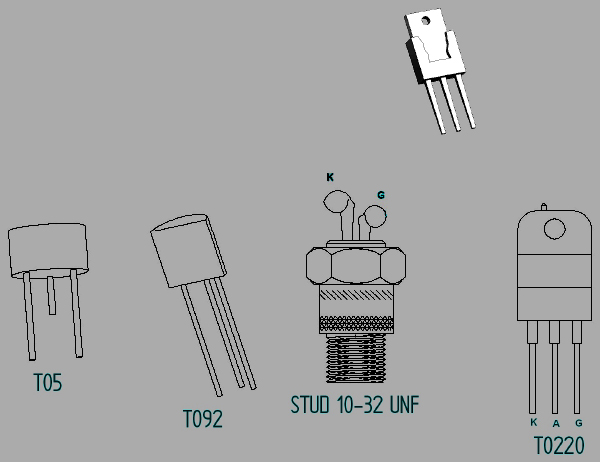
- In its off state, if the device is triggered with a pulse at the gate, then the thyrister switches from a non-conducting state into a low resistance forward conducting state. Once triggered in conduction, the thyristor remains on unless the current flowing through it is reduced below the holding current value or it is reverse-biased. The thyristor has extremely non-linear voltage-current characteristics.
- The devices can fail because of excessive temperature and high rates of temperature cycling, the failure being open circuit or short circuit between terminals. An ohmmeter can be used to check for these failures.
Testing SCR
- The PN junction from gate to cathode of SCR can be tested with an ohm meter similar to a regular diode. However, testing from anode to cathode will not indicate if an SCR is working properly, because one of the PN junctions is always reversed biased.
- The SCR can be tested with an ohm meter by placing the positive lead on the anode and the negative lead on the cathode with the gate left open. The meter should read high or infinite resistance:

Testing SCR with ohmmeter
- Placing a clip lead from the anode or positive lead of the ohm meter to the gate triggers the SCR and it should indicate low resistance.
- When the clip lead is removed, the meter continues to indicate low resistance if the power source is sufficient to produce the required holding current.
Testing DIAC
- A DIAC is basically a TRIAC without a gate terminal. It does not switch into the ON state as sharply as TRIAC.
- A DIAC can be tested with a power supply voltage that is at least a few volts greater than its break over voltage (Vbo), typically 50 V, DC:
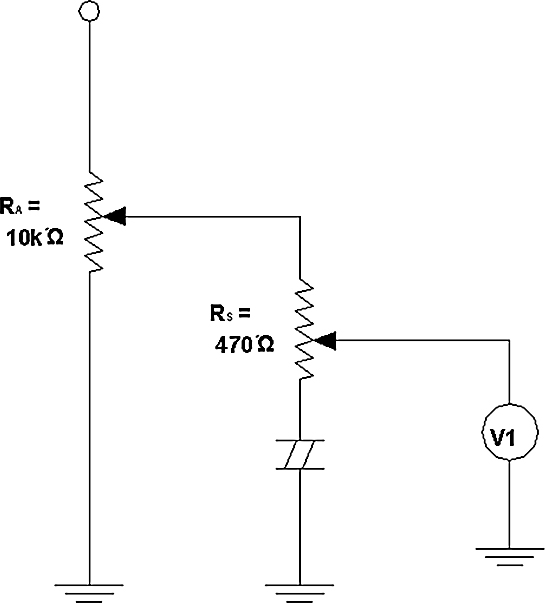
Testing DIAC
- The DIAC is connected in series with a small value limiting resistor (about 680 Ω ), which in turn is connected to a potentiometer or variable power supply voltage.
- The voltage across the circuit is increased in the circuit and the same procedure is performed to test its reverse operation. Typical break over voltage is about 30 volts and peak repetitive forward current is about 2 A.
Testing TRIAC
- The TRIAC is similar in operation to two thyristors connected in reverse-parallel, but with a common gate connection. TRIAC is a device that can pass or block current in both directions. It can be triggered into conduction in either direction by applying either positive or negative gate signals.
- A TRIAC can be tested with an ohm meter similar to testing an SCR:
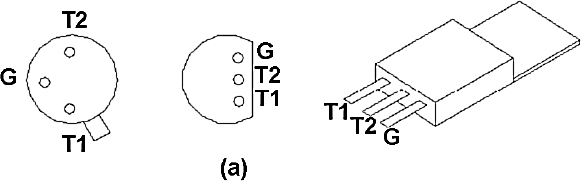
Lead identification of TRIAC
- The positive lead of the ohm meter is placed on T2 and the negative lead is placed in T1. A clip lead is placed from the positive lead to the gate, which should trigger on TRIAC. The meter should indicate low resistance.
- When the clip lead is removed, the meter continues to indicate low resistance if the power source is sufficient to produce the required holding current.
- The meter leads are reversed on the main terminals of the TRIAC and the clip lead is placed from the negative lead to the gate to test for conduction in the reverse direction.
Testing LED
- An LED is tested in the same way as a regular diode. The ohm meter will show low resistance in the forward biased condition and high or infinite resistance in reverse biased condition:
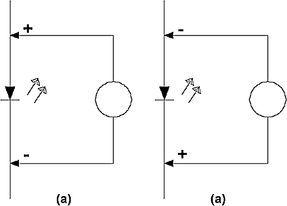
Testing LED
- The LED may even glow slightly with forward bias if the ohm meter can produce sufficient current.
- A DMM will show a higher forward drop from 1.2 to 1.5 V.
Testing Photo Detectors
- Most Photo Detectors can be tested with an ohm meter by reading the resistance of the device when the light is present and then when the light is blocked:
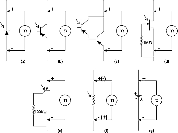
Testing Photo Detectors
- When the light strikes the photo detector, the resistance should be low and when the light is blocked, the resistance should go high or infinite.
- Using the same procedure, the voltage of a solar cell can be tested with a voltmeter.
Testing OP-AMP
Because of the infinite input impedance, no current can flow between the input terminals of the amplifier. The voltage across the input terminals of op-amp must be zero or negligibly small.
Op-amp has infinite voltage gain; it means that we get a very large voltage output from a very small voltage input. Even with a small voltage at input, the amplifier is driven into positive or negative saturation very easily.
- An operational amplifier is a very high gain operational amplifier circuit with two high-impedance input terminals and one low impedance output. The inputs are identified as inverting input and non-inverting input. It is a complete amplifier circuit constructed as an integrated circuit on a single silicon chip. Inside it contains a number of transistors and other components packed into a single functional unit.
- The basic circuit consists of a differential amplifier input stage and an emitter follower output stage. The operational amplifiers have a high voltage gain typically about 200 000.
- If the feedback resistance of the amplifier is high, then the amplifier must have a high gain in order to overcome the feedback signal opposition. The feedback signal is used to maintain the input DC voltage at zero volts. If the feedback resistance is low, then the gain is low because not much output signal is needed to feed back the common mode input in order to maintain the voltage at zero volts.
- For testing, op-amp is treated as a single device rather than breaking it into its constituent components. Op-amps are highly reliable and require little troubleshooting. They are typically low frequency amplifiers, so an oscilloscope check of the input and output signals, is the usual procedure. Look for distortion, especially clipping in the output signal.
- The characteristics of an ideal op-amp are:
- Infinite input impedance
- Zero output impedance
- Infinite open loop voltage gain
- Zero offset (voltage at output when input is zero)
- Infinite bandwidth
- Some of the major applications of op-amp are: integrator, differentiator, low pass filter, high pass filter, band pass filter, reference voltage source, voltage regulator, peak detector, comparator, logarithmic amplifier, divider, photo-cell amplifier, square wave generator, sine wave generator.
Op-amps can be tested with the help of a test jig as shown in the following figure:

Op-amp Test Circuit
- The circuit consists of an oscillator which is built around the op amp.
- Let us take an op-amp IC 741. This IC is connected to an oscillator circuit as shown. This oscillator circuit operates on the signals generated by the op-amp. LED is connected to the output of the oscillator circuit.
- If the op-amp is good, the oscillator circuit will work, which is indicated by the flashing LED. The oscillating frequency is 2 KHz.
Circuit Stability Precautions
- The operational amplifier circuit can become unstable because of load capacitance and stray capacitance. For large load capacitances there can be specialized compensation circuits recommended by the device manufacturers. Stray capacitances can best be avoided by good circuit construction techniques. However, the effect of stray capacitance also depends upon the resistor values in a feedback network.
- High resistance values make the circuit more susceptible to instability caused by stray capacitances. Hence a low resistance feedback network helps ensures circuit stability.
- Feedback along supply lines is another source of op-amp circuit instability. This can be minimized by connecting 0.01μF high frequency capacitors from each supply terminal to ground:

Op-amp circuit stability
- The capacitors must be connected as close as possible to the IC terminals. The following precautions are required for op-amp circuit stability:
- For low frequency circuit performance, use an internally compensated op-amp like 741.
- To bypass the supply terminals to ground use a bypass capacitor of 0.01μF.
- The signal source which is connected to the circuit must be tested.
- Do not connect oscilloscope or other instruments at the input terminals (inverting and non-inverting) of op-amp. The input capacitance of the instrument can cause instability.
- Even after taking all of the above precautions, if the circuit is still unstable, reduce the value of all circuit resistors except compensating resistor. If possible, also reduce the signal source resistance.
Testing Timer IC555
- The 555 is a monolithic timing circuit that can produce accurate and highly stable time delays or oscillation. The timer basically operates in one of the two modes: either as a monostable (one shot) multivibrator or as an astable (free running) multivibrator.
- The device is available as an 8-pin metal can, an 8-pin mini DIP or 14-pin DIP. The important features of this IC are:
- It operates on +5V to +18V supply voltage in both astable and monostable modes.
- It has adjustable duty cycle; timing is from microseconds to hours.
- It has a high current output; it can source or sink 200mA current.
- The output can drive TTL and has a temperature stability of 0.005 % per ˚C.
- It is reliable easy to use and low cost.
- Applications of IC555 are monostable and astable multivibrators, waveform generators, analog frequency meters and tachometers, temperature measurement and control, infrared transmitters, burglar and toxic gas alarms, voltage regulator and many more.
IC 555 can be tested with a test jig as shown in figure 4.21:
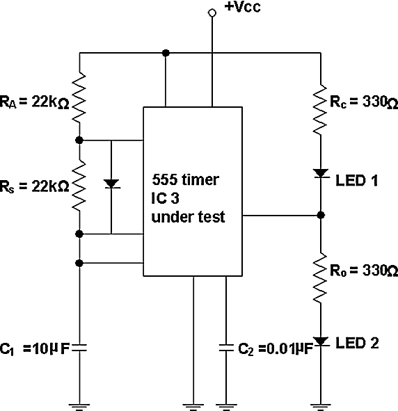
555 IC Timer Testers
- Its output frequency is about 3 Hz. When the output is low, LED1 lights, and when the output is high, LED2 lights.
- This is only a functional test indicating that the output can turn on and off, which is usually sufficient to prove that the 555 timer under test is functioning.
- It does not indicate if some of the components within the IC have changed their values, which could affect its precision operation. Only an exact replacement in an actual can determine this.
- This tester can be mounted on a small perforated board using an IC socket and a 9 V battery.
4.5 Testing Diodes, Transistors and In-Circuit Semi-Conductors Using Oscilloscope
- Set the oscilloscope in component testing mode. The general conventions for the CT mode as explained earlier are to be followed.
- Connect the terminals of the device to the test terminals.
- Compare the pattern obtained with the corresponding pattern as shown in the following figures:
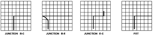
Test Patterns for single Transistor

Test Patterns for single Diode

Test Patterns for in-circuit semiconductors
4.6 Switches
In electronic systems, switches are used to make a particular function (like power) either be ON or OFF. There are only two active states of a switch: ON and OFF. These two states are achieved with the help of two pieces of metal which are known as contacts. These contacts touch to make a circuit and separate to break a circuit. The common types of switches used in electronic equipment are as follows:
- Toggle Switch
- Push-button switch
- Micro switch
Let us address these one by one:
Toggle Switch
This is the most popularly used switch in electronic systems. The meaning of toggle switch is that it can be turned ON when pressed and it springs back to OFF when released. The various versions of toggle switch are:
Single Pole Single Throw (SPST)
Here the two terminals are either connected together or not connected to anything.
Single Pole Double Throw (SPDT)
It is a simple changeover switch where the contacts can be made with either of the two terminals.
Double Pole Single Throw (DPST)
It is equivalent to two SPST switches together, which are controlled by a single mechanism.
Double Pole Double Throw (DPDT)
It is equivalent to two SPDT switches together, which are controlled by a single mechanism:
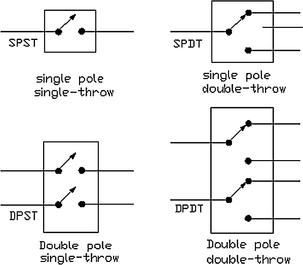
Types of toggle switches
These switches are used where a reset or preset pulse is required. A pole is a set of contacts that belong to a single circuit. A throw is one of two or more positions that the switch can adopt.
Push-button Switch
It is similar in action to toggle switch. Many times it incorporates a lamp indicator under the pushing surface.
In this type, there is a holding coil which latches the switching ON position when depressed. When the switch is pressed for the second time, it releases the voltage from the holding coil and returns the switch to its OFF condition.
Micro switch
It is spring loaded switch and is often placed in a drive unit so that closing its contacts causes its cycle to repeat or stop. In other words, when the switch is operated, it causes change in operation.
Troubleshooting of Switches
Usually a defective switch is not repairable. It is recommended to replace the broken or defective switch. The defects in a switch can be loss of continuity between the contacts, improper spring loading function because of a defective spring, loose toggle, broken or burnt switch body, and so forth.
In order to make an in-circuit test on a switch a VOM can be employed. The following figure shows how to use a VOM for this purpose:

Testing a switch
The meter prods are connected or touched to both the sides of switch. The meter shows infinite resistance when the switch is in OFF position.
When the switch is closed, i.e. ON, the meter shows zero resistance indicating that the two sides of the switch are electrically connected.
If the switches are found to be faulty, replace the switch. Carefully switch off the power while replacing it. If there are any connections made to the switches, label all the wires connected to it before removing. When the new switch is replaced, connect all the wires in their proper positions. Turn on the power and check the working of the switch by the procedure described above.
4.7 Safety Issues for plugs, sockets and portable appliances
Portable Appliance Testing (commonly known as PAT or PAT Inspection or PAT Testing) is a process in the United Kingdom, New Zealand and Australia by which electrical appliances are routinely checked for safety. The correct term for the whole process is In-service Inspection & Testing of Electrical Equipment.Test and tagging is a generic name given to the process of visually inspecting and electrically testing in-service electrical equipment for personal use and/or safety The aim of test and tagging is to determine if the appliance is electrically safe for personal use. The appliance undergoes a visual inspection for defects such as damage or missing components and a number of electrical tests to measure earth continuity, insulation resistance and polarity.
In Australia and New Zealand, this is done using the Standard; AS/NZS 3760:2010 “In-service inspection and testing of electrical equipment” as a reference document.
The tests an appliance is required to undergo will depend on the type of appliance, it’s electrical Class and subject to a risk assessment by the technician. The tests normally done under PAT testing are:
- Earth Resistance Test
- Earth continuity test
- Insulation resistance test
- Polarity check
4.8 Summary
Passive components like resistors, capacitors and inductors can not amplify or oscillate a signal.
A diode can be conveniently checked with an OHM METER by measuring its forward and reverse resistance. A signal diode shows a low resistance (a few hundred ohms) in the forward direction and a high resistance (nearly infinity) in the reverse direction.
In a bipolar transistor, shorting base to emitter turns off transistor, while forward biasing base-emitter junction turns on transistor. Shorting collector to emitter simulates saturation, as the transistor behaves like a closed switch.
JFET and MOSFET are the two types of FET which are again divided into n-channel and p-channel. The basic functionality of the field effect transistors can be checked by assuring the flow of current from source to drain.
Special care has to be taken while dealing with MOSFET. The SiO2 layer which is very thin may rupture even because of the static charges.
In today’s electronic world Digital Integrated Circuits are used extensively. There is hardly any area in which digital circuits are not used. The digital circuits operate from defined voltage levels which give a certain defined output. The systems which employ mainly digital circuits have predictable behavior of the circuit.
The basic elements of all digital circuits are logic gates that perform logical operations on their inputs.
Learning objectives
- Understand the difference between analog and digital signal
- Study what is digital troubleshooting
- Know the typical faults in digital circuits
- Study digital troubleshooters
- Study of PLD and Memory
- Understand the troubleshooting of RAM and ROM
5.1 Moving from Analog to Digital
Difference between Analog and Digital Signals
Information carrying signals are divided into two broad classes:
- Analog Signal
- Digital Signal
Analog Signals are continuous where digital signals are discrete. Analog signals are continuously varying where digital signals are based on 0’s and 1’s.
Analog signals are continuous electrical signals that vary in time. The variations follow the original signal, showing that the two are analogous. Hence the name is analog.

Analog Signal
In the above analog or continuous signal, voltage is defined for all time instances.
Digital signals consist of pulses or digits with discrete levels or values. The value of each pulse is constant, but there can be an abrupt change from one digit to the next. A digital signal uses some physical property, such as voltage, to transmit a single bit of information.
Suppose we want to transmit the number 6. In binary, that number is 110. We first decide that, say, a “high” means a 1 and “low” means a 0. Thus, 6 might look like:
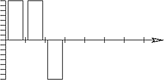
Digital Signal
In the above digital signal, voltage is defined at integer time instances.
Examples:
- Analog: Telephone voice signal is analog. The voice intensity causes electric current variations. The signal is reproduced at the receiving end.
- Digital: A simple or scientific digital calculator is the best example of a digital system whose input as well as output is in digital form.
The information can be represented in terms of some form of analog or digital signal. The digital data stored on a CD will normally have been produced using analog to digital converters.
In fact, Analog and Digital signals are no more than mathematical representations of a signal, which is useful when we want to process information.
Why Digital circuits?
- Digital integrated circuits are used extensively in all branches of electronics, communication systems and medical equipment.
- Digital circuits operate from defined voltage levels, which reduces any uncertainty about the resulting output and behavior if the circuit.
- Many circuits operate with voltages that can only be either ‘on’ or ‘off’. For example a light can be switched on or off, a motor can be running or stopped, all these are digital operations with only two states and would need digital circuit elements for their operation and control.
- The basic elements of all digital circuits are logic gates that perform logical operations (AND, OR etc) on their inputs.
5.2 Moving into the Digital Circuits
Digital circuits cover a wide range from high current industrial motors to microprocessors. However, the basic elements of all digital circuits are logic gates that perform logical operations on their inputs. Therefore, it is essential to understand the basics of logic gates before discussing troubleshooting techniques.
Truth Table
The truth table lists all the possible things that can happen at the input and output terminals. Any logic device can be explained with the help of a truth table. It is a tabular explanation of the logic device which represents its output side for any set of inputs. Following is an example of truth table:
Truth Table
| Input States | Output States | |
| A | B | |
| 0 | 0 | 0 |
| 0 | 1 | 0 |
| 1 | 0 | 0 |
| 1 | 1 | 1 |
So there is an input stage and output stage. The above logic circuit has two inputs A and B. Depending upon the combination of these two inputs, the output changes. It is not necessary that these inputs will always be zeroes and ones. The following table shows the other possible things which they can represent:
Other Possibilities
| Motor | Not running = 0 | Running = 1 |
| Lamp | Off = 0 | ON = 1 |
| Tape Recorder | Not recording = 0 | Recording = 1 |
| TV set | Off = 0 | ON = 1 |
| Relay | Not energized = 0 | Energized = 1 |
| Transistor | Cut off = 0 | Saturated = 1 |
| Voltage | 0V = 0 | 5V = 1 |
| Door | Open = 0 | Closed = 1 |
There can be a number of logic states. The following table shows some examples:
Logic States
| 0 | 1 |
| Open | Closed |
| Positive | Negative |
| True | False |
| ON | OFF |
| Positive | Negative |
Two-state operation is widespread in digital electronics because it is the most reliable way to operate transistors and other switching devices. With two state operations all the signals are easily recognizable as either high or low.
The AND Gate
In the following figure there are only two inputs A and B and one output X. So it is known as a two input AND gate. It is possible for the AND gate to have more inputs, but there is only one output terminal:

AND gate: equivalent circuit and schematic symbol
Referring to the equivalent circuit, only when, A and B switches are closed simultaneously, there can be an output, i.e. when the power is applied both the switches must be closed before the lamp X will light:
Truth Table of AND gate
| A | B | X |
| 0 | 0 | 0 |
| 0 | 1 | 0 |
| 1 | 0 | 0 |
| 1 | 1 | 1 |
The truth table shows that there is only one way to get logic 1 at output. That is all the inputs must be at logic 1 level to get logic 1 output.
In digital electronics, the AND gate is used as a control element with one input regulating the traffic through others. When the presence of two or more factors is necessary to produce the desired result, the AND gate is employed.
The OR Gate
The equivalent circuit shows that the switches A and B (inputs) are connected in parallel. There will be an output X, whenever there is logic 1 at either or both the inputs. If either or both the switches is closed, power will be applied to the lamp and then it will glow:
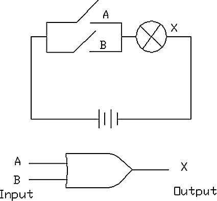
OR gate: equivalent circuit and schematic symbol
Truth Table of OR gate
| A | B | X |
| 0 | 0 | 0 |
| 0 | 1 | 1 |
| 1 | 0 | 1 |
| 1 | 1 | 1 |
The truth table shows that there is only one way to get logic 0 at output. That is all the inputs must be at logic 0 level to get logic 0 output. In order to get logic 1 output, either or both the inputs must be at logic 1.
In digital electronics, the OR gate provides the means of achieving a desired result with a choice of two or more inputs.
The NOT Gate
With this type of gate the output is always opposite of input. In the relay circuit shown below, the lamp X is ON whenever the circuit is not energized. That is, whenever the switch A is open, the lamp glows. When the switch A is closed, the relay is energized and the lamp is OFF:
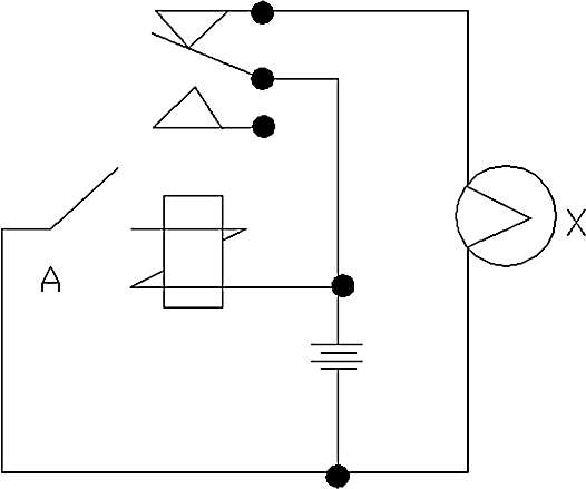
NOT gate (a) relay circuit
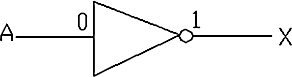
(b) Schematic symbol
Truth Table of Inverter
| A | X |
| 1 | 0 |
| 0 | 1 |
The truth table shows that output is always opposite of input, irrespective of the logic state of input. It is also known as an ‘inverter’ gate. It is applied if it is necessary to change the state of information before it is used.
Most of the times, the inverter is used in conjunction with another logic element. In that case it is represented by a small circle directly connected to the other logic element.
The NAND Gate
The gate is negated AND gate. The NOT gate and the AND gate can be combined together to get a NAND gate.
In the following figure there are only two inputs A and B and one output X. So it is known as a two input AND gate. It is possible for the AND gate to have more inputs, but there is only one output terminal:
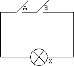
NAND gate (a) equivalent circuit

(b) Schematic symbol
Referring to the equivalent circuit, the switches A and B (inputs) are connected in series and this series combination is connected in parallel to a lamp X (output). In order to make the lamp ON, at least one switch must be open:
Truth Table of NAND gate
| A | B | X |
| 0 | 0 | 1 |
| 0 | 1 | 1 |
| 1 | 0 | 1 |
| 1 | 1 | 0 |
The truth table shows that if any one of the inputs is logic 0, the output is logic 1. When both the inputs are logic 1, the output is logic 0.
The NOR Gate
The NOR gate can be obtained by inverting the output of an OR gate, which produces a ‘NOT OR’ gate.
In the equivalent circuit, the two switches A and B (inputs) are connected in parallel with the lamp X (output), as shown. The lamp glows, only if all the switches are left open:
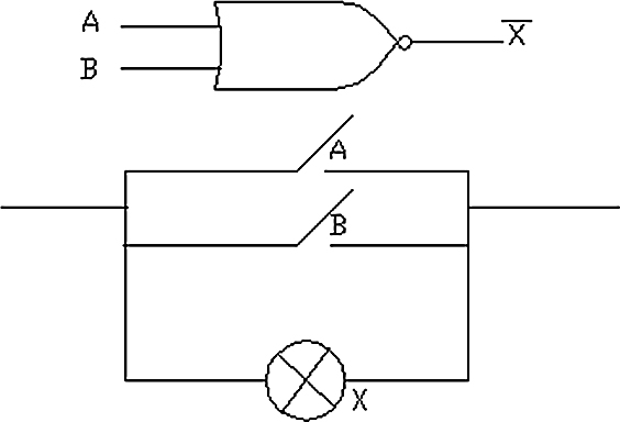
NOR gate: schematic symbol and equivalent circuit
Truth Table of NOR gate
| A | B | X |
| 0 | 0 | 1 |
| 0 | 1 | 0 |
| 1 | 0 | 0 |
| 1 | 1 | 0 |
The truth table shows that when both the inputs are at logic 0 levels, then only the output is logic 1, otherwise for all the other combinations the output is logic 0.
The EX-OR Gate
It is known as Exclusive OR gate. It can be regarded as a combination of AND and OR gate. The equivalent circuit is as shown in the following figure. The two switches A and B (inputs) are connected as shown. The lamp X glows only when one switch is ON and the other is OFF. The lamp does not glow when both the switches are in same condition, such as either ON or OFF:
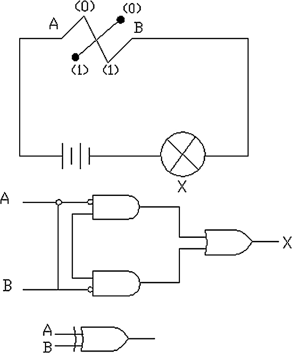
EX-OR gate equivalent circuit and schematic symbol
Truth Table of EX-OR gate
| A | B | X |
| 0 | 0 | 0 |
| 0 | 1 | 1 |
| 1 | 0 | 1 |
| 1 | 1 | 0 |
The truth table shows that when both the inputs are at logic 0 levels or logic 1 levels, then the output is logic 0, otherwise the output is logic 1.The EX-OR gate can be used to compare the inputs. It gives zero output whenever the inputs are matched. When the inputs are the same, it gives positive output.
The EX-NOR Gate
It is known as Comparator gate. It can be regarded as a combination of AND and OR gate. The two input comparator gate is a combination of one AND gate and two OR gates as shown in the configuration:
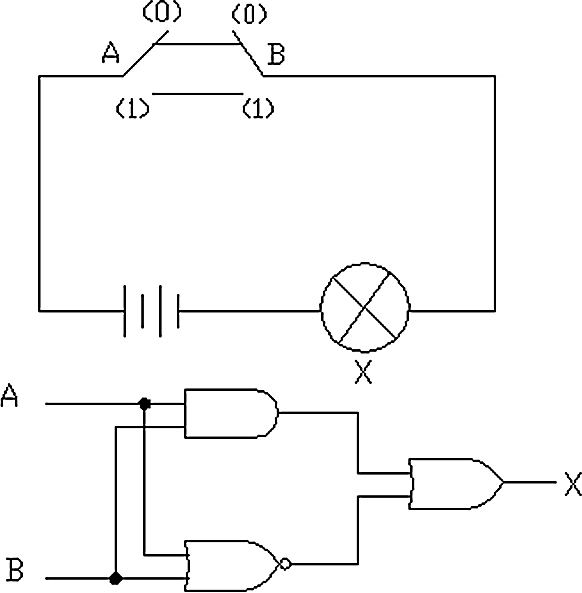
EX-NOR gate: equivalent circuit and configuration
The output of comparator will stand at defined ‘1’ state only if all the inputs stand at their defined ‘1’ states or if none of the inputs stand at its defined ‘1’ state.
Truth Table of EX-NOR gate
| A | B | X |
| 0 | 0 | 1 |
| 0 | 1 | 0 |
| 1 | 0 | 0 |
| 1 | 1 | 1 |
The truth table shows that when both the inputs are at logic 0 levels or logic 1 levels, then the output is logic 1, otherwise the output is logic 0. The EX-NOR gate can be used to compare the inputs. It gives positive output whenever the inputs are matched. When the inputs are not same, it gives negative output.
The INHIBIT Gate
It is an OR gate with an inhibiting input. Here, the output is at its ‘1’ state if and only if the inhibit input stands at its defined ‘0’ state AND one or more of the normal OR inputs stand at their defined ‘1’state:
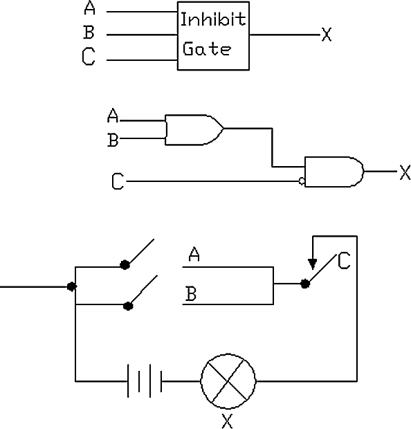
EX-OR gate: graphical representation, configuration and equivalent circuit
Truth Table of INHIBIT gate
| A | B | C | X |
| 0 | 0 | 0 | 0 |
| 1 | 0 | 0 | 1 |
| 0 | 1 | 0 | 1 |
| 1 | 1 | 0 | 1 |
| 0 | 0 | 1 | 0 |
| 1 | 0 | 1 | 0 |
| 0 | 1 | 1 | 0 |
| 1 | 1 | 1 | 0 |
The truth table and the configuration shows that when C input (inhibit) is zero AND any one of the normal OR inputs A and B is 1 , then only the output X is at logic 1 state, otherwise it is at logic 0 state.
This gate is very useful for controlling inputs (A and B) by means of the inhibiting signal C. When the inhibiting signal is present (C = 1), the output is always OFF (X=0), but when the inhibiting signal is absent (C = 0), the signals (A and B) can pass through the output.
Digital IC Logic Families
The digital circuits are invariably constructed with ICs. Digital IC gates are classified not only by their logical operation but also by their specific logic circuit family to which they belong. Each logic family has its own basic electronic circuit upon which more complex digital circuits and functions are developed. The basic circuit in each family is either a NAND or a NOR gate. The electronic components employed in the construction of the basic circuit are usually used to name the logic family. There are many families of digital ICs. The popular logic families are discussed below:
TTL – Transistor-transistor logic
ECL – Emitter-coupled logic
MOS – Metal-oxide Semiconductor
CMOS – Complementary Metal-oxide Semiconductor
- The most popular and most widely used logic family is the TTL family. It has an extensive list of digital functions. The basic element used in TTL circuits in the bipolar transistor. It makes use of a multiple-emitter transistor for the input device. TTL ICs are usually distinguished by numerical designation as the 5400 and 7400 series.
- There is one more family called Schottky TTL. In this family the gates are faster than standard TTL because there is a reduction of propagation delay, but results in an increase in power dissipation. They are available in the numerical form as 74S / 54S series. 74LS / 54LS are low power Schottky TTL series.
- In ECL family there are less logic swings as compared to TTL. The reason behind this is that the transistors, when conducting are not saturated. The most common ECL type is designated as the 10,000 series. For example, the 10102 provides the four 2-input NOR gate. The ICs belonging to this family have a higher speed than the gate.
- The MOS and CMOS logic families are widely preferred over TTL and ECL. The characteristic feature of this family is low power dissipation and good noise immunity. These two families are used for LSI (Large Scale Integration) functions. The great advantage of CMOS technology is high density packing of a large number of devices. CMOS circuits come in 4000 series. For example, a quad-2-input NOR gate has the number 4001.
Logic Signal Voltage Level
- Logic gate circuits are designed to input and output only two types of signals: “high” (1) and “low” (0), as represented by a variable voltage: full power supply voltage for a “high” state and zero voltage for a “low” state. In a perfect world, all logic circuit signals would exist at these extreme voltage limits, and never deviate from them (i.e., less than full voltage for a “high,” or more than zero voltage for a “low”). However, in reality, logic signal voltage levels rarely attain these perfect limits due to stray voltage drops in the transistor circuitry, and so we must understand the signal level limitations of gate circuits as they try to interpret signal voltages lying somewhere between full supply voltage and zero.
- TTL gates operate on a nominal power supply voltage of 5 volts, +/- 0.25 volts. Ideally, a TTL “high” signal would be 5.00 volts exactly, and a TTL “low” signal 0.00 volts exactly. However, real TTL gate circuits cannot output such perfect voltage levels, and are designed to accept “high” and “low” signals deviating substantially from these ideal values. “Acceptable” input signal voltages range from 0 volts to 0.8 volts for a “low” logic state, and 2 volts to 5 volts for a “high” logic state. “Acceptable” output signal voltages (voltage levels guaranteed by the gate manufacturer over a specified range of load conditions) range from 0 volts to 0.5 volts for a “low” logic state, and 2.7 volts to 5 volts for a “high” logic state:
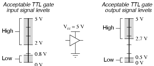
Acceptable TTL gate signal levels
- If a voltage signal ranging between 0.8 volts and 2 volts were to be sent into the input of a TTL gate, there would be no certain response from the gate. Such a signal would be considered uncertain, and no logic gate manufacturer would guarantee how their gate circuit would interpret such a signal.
- CMOS gate circuits have input and output signal specifications that are quite different from TTL. For a CMOS gate operating at a power supply voltage of 5 volts, the acceptable input signal voltages range from 0 volts to 1.5 volts for a “low” logic state, and 3.5 volts to 5 volts for a “high” logic state. “Acceptable” output signal voltages (voltage levels guaranteed by the gate manufacturer over a specified range of load conditions) range from 0 volts to 0.05 volts for a “low” logic state, and 4.95 volts to 5 volts for a “high” logic state:
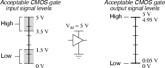
Acceptable CMOS gate signal levels
- It should be obvious from these figures that CMOS gate circuits have far greater noise margins than TTL: 1.45 volts for CMOS low-level and high-level margins, versus a maximum of 0.7 volts for TTL. In other words, CMOS circuits can tolerate over twice the amount of superimposed “noise” voltage on their input lines before signal interpretation errors will result.
Basic Digital Troubleshooting
- The first step in learning digital troubleshooting is to learn the components that are available, and what is the overall functionality of the component in the circuit.
- The second step is to study basic circuits that are made from the components. The basic logic components in digital circuits are Logic gates (AND, OR, and NOT gates) and basic logic circuits are Flip-flops and so on.
- The third step in learning digital troubleshooting is to study how the basic circuits are combined into a complete system. For example, Counter, can be a digital system.
- Apart from this, one must also know how to conduct tests and measurements, and recognize symptoms.
- A logic circuit can have three basic signals:
- Logic 1; it is just a way to refer the higher voltage level
- Logic 0; it is the lower voltage level
- A pulsating voltage signal that alternates between 0 and 1
- The quickest and most convenient way to measure these signals is to use a logic probe, not a voltmeter. An LED is used as an indicator and a series resistor to limit the current flowing through LED. The following figure shows a drawing of a logic probe:

A basic logic probe
- When the probe is touching a 1 signal, the LED is ON, and when it touches a 0 signal, the LED is OFF. When it touches a pulsating signal, the LED is ON at half brightness or it is flashing ON and OFF. The following figure shows symbols for different logic probe indications.
- A logic probe is better than a voltmeter in digital troubleshooting. It is not required to take a reading each time when the probe is set. For example, suppose the voltmeter is in a circuit where 4.5 V is a logic 1 and 1 V is a logic 0 signal. If a voltmeter indicates 2.5 V, it does not mean that you are looking at low 1 signal or high 0 signal or a pulse. But with a good logic probe this guesswork is eliminated.
5.3 Typical Faults in Digital Systems
These can be some of the reasons for the faults to get induced in any digital circuit:
- Breaks in PCB tracks
- Shorts between tracks on the PCB
- Failure of discrete components external to the IC
- Dry joints
The typical failures include inputs or outputs shorted to ground, pins shorted to Vcc supply, pins shorted together, open pins and connections with intermittent defects.
There are hundreds and thousands of semiconductor devices assembled on one small chip. The critical problem for the chip manufacturers can be to get the voltages and signals in and out of such a tiny chip.
The wires which are used as inputs and outputs to the chips are very thin. Any type of thermal stress can affect these tiny wires and the bond may break away from the pad to the chip, causing an open connection.
The faults in a gate output manifest themselves as follows:
- Stuck at ‘1’, i.e. always above 2 V irrespective of input state (for TTL):

Output stuck at ‘1’ (for a single gate)
In the above figure the output is stuck at ‘1’ whereas with logic ‘1’ on inputs the output should be less than 0.8 V. The possible faults in this circuit could be internal transistor open circuit or 0 V line open circuits internally.
- Stuck at ‘0’, i.e. always less than 0.8 V irrespective of input state (for TTL):
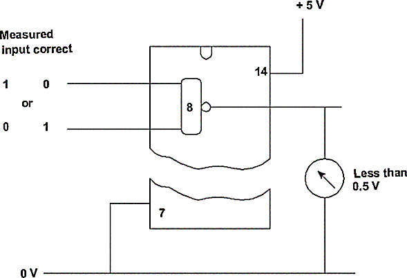
Output stuck at ‘0’ (for a single gate)
Here the output is stuck at ‘0’ whereas it should be logic ‘1’. The possible faults in this gate could be a short-circuited internal transistor, or Vcc line internally open.
- High impedance state output, i.e. output not 0 or 1.
The causes of the above faults are possibly due to internal IC failure. The internal failures can be of the following type:
- There can be a short circuit between an input terminal or an output terminal to Vcc or to the ground.
- There can be a short circuit between two pins, neither of which is at Vcc or ground potential.
- There can be an open lead which could be either an input or an output pin.
5.4 Digital Circuit Troubleshooters
- Analog test equipment are not recommended for troubleshooting of digital circuits. The digital circuits have only two narrow voltage ranges, high and low, which represent logic ones and zeroes.
- The process of analyzing faults in a digital circuit is by sequentially operating gates and ICs within the system and then comparing the resulting outputs with those which should be normally present. This can be done by suitable test signals and checking the resulting operations by suitable displays.
- Many types of digital test aids are available, some of which are described below.
Logic Clip
- It is a simple instrument which is easy to use and handy to carry. It clips on any TTL or CMOS IC. It helps to observe 16 pins of an IC at a glance.
- The logic clip is clipped to an IC where it makes contacts with each pin of IC. It shows the status of each pin via an individual LED:
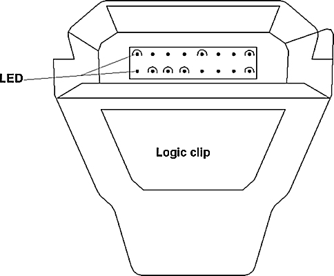
Logic Clip (model 548A from HP Co
- This feature is particularly useful in sequential logic devices such as counters and shift registers or with any circuit with a truth table that needs checking.
- Each of the clip’s 16 LEDs independently follows changes at its associated pin. The display on the logic clip shows logic high (LED on), logic low (LED off) and pulse activity (LED dim ).
- It has no controls to set and no power connections.
Logic Probe
- The logic probe provides a simple means of digital troubleshooting by detecting voltage levels or pulses at a given point and provides functional indications of in-circuit logic activity.
- It uses a single lamp (LED) as an indicator which indicates various states possible on a digital signal path i.e. high, low, single pulse, pulse train, open circuit:
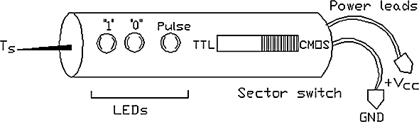
Logic Probe
- The above figure shows an HP’s 545A Logic Probe. The lamp indicator allows 360 degrees viewing to clearly and quickly show the state of the circuit under test. This logic probe allows CMOS to TTL selectable operation. When switched to TTL position, it operates from 4.5 to 15 V dc power supplies. In CMOS position, logic threshold levels are variable from 3 to 18 volts.
- A typical indication format is:Lamp ON —— High
Lamp OFF ——Low
Lamp DIM —— Open or bad level
One flash ——Single pulse
Repetitive flashes —– Pulse Train - An important feature of the logic probe is its ability to stretch pulses so that short, fast pulses are slowed down and lengthened at the display making them easy for the operator to see. For example a 10 ns pulse is stretched to 100 ms so that the user can see it. This is accomplished by using the leading edge of a short pulse to trigger a circuit whose time delay is 100 ms.

Logic probe response to various digital signals
- An auxiliary unit to logic probe is the pulse memory unit which is capable of capturing and displaying transient pulses, which are otherwise hard to see. When the probe tip detects such a pulse, it is stored in the memory. Use of the memory causes no change in probe operation.
- Some logic probes have two LED display indicators: a green LED for logic 0 and a red for logic 1.
Logic Pulser
- A Logic Pulser is used to stimulate digital circuits and supplemented by a logic probe it aids in testing for circuit response to easily check gates, lines, buses and nodes. It does the same job in digital systems as a signal generator does in analog systems. It injects a desired signal for the purpose of testing:
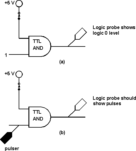
Logic Pulser determines gate operation
- The above figure shows a troubleshooting problem where a combination pulser and probe can save time by preventing a wrong interpretation of a measurement.In figure (a), the logic probe shows a logic 0 output of the AND gate which should be logic 1.
Figure (b) shows how to test for this problem. The pulser injects the signal and the logic probe is used to look for that signal. - If the problem is with the gate, the probe will show a pulse signal. If the point is grounded, the probe will indicate no signal:

Logic Pulser
- Pulse height or amplitude is derived from the power supply that the pulser is connected to. For this reason the pulser should always be powered from the circuit under test or power supply from the same voltage.
- The power supply requirements of the pulser are 3 to 18 V dc for CMOS and 4.5 to 5.5 V dc for TTL.
Logic Current Tracer
- Current tracing is a very effective form of troubleshooting. It is difficult to isolate a bad element when a given circuit node is stuck in one logic state and several elements are common to that node. The hand held current tracer has one lamp indicator that glows when it is held over a pulsing current path.
- The instrument detects whether current is flowing or not and where the current is flowing. For instance if the node is stuck on LOW state due to a shorted input in one of the devices connected to the node, a very strong current exists between the circuit driving the node and the faulty component.
- The use of a current tracer helps to pinpoint the faulty point on a node, even on multi layer boards.
- The current tracer senses the magnetic field generated by fast rise time current pulses in the circuit (or, provided by a logic pulser), and display steps, single pulses, and pulse trains using a simple one light indicator:
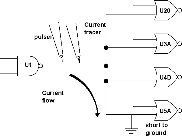
Multiple input fault detection using current tracer and logic pulser
- The above figure shows the location of a multiple input fault. Logic pulser is used to provide current pulses. Gate U5A is shorted to ground causing the node to be stuck LOW and sinking virtually all current from U1 and other inputs. A current tracer quickly verifies this fault by a clear single lamp indicator on the node.
- Current pulser is also used for the following conditions:
- A solder bridge fault can be detected using a current tracer:
Figure 5.22
Solder bridge faultIn the above figure a solder bridge between U1 and U2 causes both nodes to indicate functional logic failures. Tracing current flow in the circuit quickly shows the location and cause of the fault.
- A solder bridge fault can be detected using a current tracer:
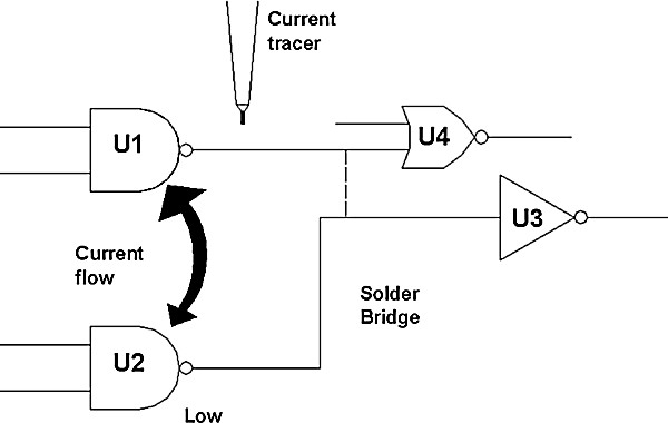
- If a node has been identified on which the voltage is stuck high or low, then it is important to isolate whether the driver is dead or something like a shorted input is pushing the node to a fixed value. A current tracer is used in such a condition. If the driver is dead, the only current indicated by the tracer will be that caused by parasitic coupling from ant nearby currents, which are very small:
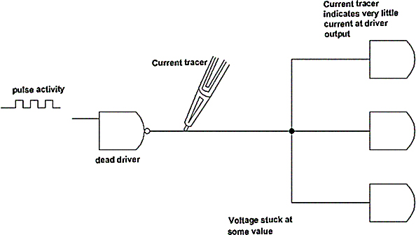
Stuck node
- If the driver is good, a normal short circuit current will be present and can be traced to the circuit element node.
- A current tracer can be used along with the logic pulser to locate VCC to ground short. The reason for VCC to ground short is a faulty capacitor. A shorted decoupling capacitor is also one of the major reasons of the short:
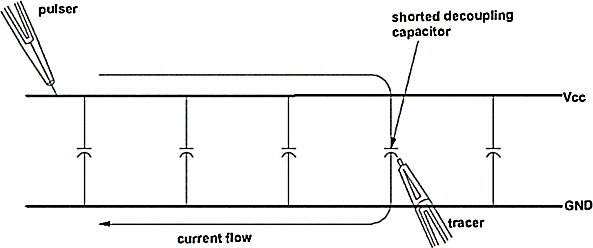
Vcc to Ground fault
- The logic pulser is used to pulse the power supply terminal. The above figure shows that the capacitors are connected between VCC and ground. The current tracer is placed at various points near the capacitors. The current tracer reveals the path which carries the greatest amount of current, i.e. the shorted path.
Logic Comparator
- A logic comparator clips onto powered TTL or DTL ICs and detects functional failures by comparing the in-circuit test IC with a known good reference IC. The comparator performs this function by comparing the output response of a reference IC against an in-circuit test IC and displaying the subsequent errors pin by pin. The IC output pin that does not correctly follow its inputs will produce an error indication, even when the error is as short as 200 ns.
- Any difference in the operation is displayed as an error by the individual LED associated with the output pin. The comparator is accompanied with a switch programmable socket board that accepts 8, 14 or 16 pin ICs. The reference IC is placed on the socket and outputs of the particular IC to be tested and is selected through 16 miniature switches which tell the comparator which pins of the reference IC are inputs and outputs:
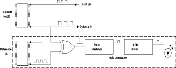
IO pin configuration
- The socket board senses which of the input pins are supply and ground, and displays output errors greater than 300 ns.
Logic Analyzer
- A Logic Analyzer is a device used to test and diagnose an electronic system, which includes an oscilloscope for displaying various digital states.
- The Logic Analyzer is a powerful development tool for use in digital systems. It is essential in system design and troubleshooting especially in vital areas of hardware timing analysis and hardware/software integration.
- The logic probes have a limitation: that is it can only be used to probe one node at a time. When it is required to simultaneously observe instantaneous status and transitions at several nodes, a logic analyzer is the correct choice.
- A logic analyzer can perform state and timing analysis on the same channel. It can also perform in-depth analysis of software and hardware problems.

Logic Analyzer
- In state analysis mode, captured data may be displayed as a list (a binary table), map or graph, while in timing analysis mode; it is displayed as a multi channel logic timing diagram. Once the desired display is obtained, a particular class of problems can be solved.
- Some logic analyzers are capable of displaying zeroes and ones instead of timing diagrams types of waveforms.
5.5 Digital Integrated Circuits
Modern electronic equipment makes use of digital integrated circuits which are in very high demand. Usually the digital integrated circuits come in dual-in-line packages. An IC can be identified from the information given on the IC itself. On its surface an IC carries the following markings:
- Manufacturer’s logo.
- Date code e.g. 7932 (79 is the year of manufacture, 32 is production batch).
- Core number e.g. 74LS51 First two numbers indicate that the IC is a member of the 7400 series IC family. The last letters give the function of IC. Letters inserted in the core of the number indicate logic subfamily. The following letters are used to denote other subfamilies:
- C: CMOS
- S: Schottky
- L: Low Power
- LS: Low Power Schottky
- H: High Speed
- A prefix to the core number identifies the manufacturer, e.g. SN 74LS51, here SN shows a device from Texas.
- A suffix indicates package type, temperature range etc. e.g. SN 74LS51 N, here N indicates the package type.
There is a white dot or a notch on the IC which indicate the orientation. Pin number 1 is always the upper left hand pin on the end of the IC that includes the notch. The pin numbers up down the left side of the IC and up the right side.
Common Faults in IC
The following types of common faults are observed in an IC:
Open Input/Output Bond:
If the output if an IC is open, it is floating. Let us consider that this output is supposed to be given as an input to another IC. In TTL circuits a floating input rises to approximately 1.5V and usually has the same effect on the circuit operation as a high logic level. This means that an open output bond in an IC will cause all inputs driven by that output to an incorrect level which are usually treated as logic high level by the inputs.
If there is an open input bond inside an IC, the digital signal that drives the signal will be unaffected and will be detectable at input pin. It will be as though the input were at the static high level.
Short Circuit between input/output and VCC or ground:
When there is a short circuit between input/output and VCC or ground, all signal lines connected to that input/output are held either high (in case of short to VCC )or low (in case of short to ground ). Thus, a fault usually causes normal signal activity at points beyond the short circuit to disappear and can be detected easily.
The following figure shows some common faults in a digital IC:
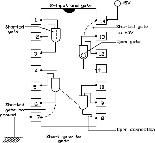
Common in a digital IC
The faults are listed as follows:
- Shorted gate to + VCC
- Open gate inside
- Shorted gate inside
- Open connection to the pin
- Short between gate to gate and
- Short between gate and ground
Troubleshooting of Integrated Circuits
Troubleshooting of the logic ICs can be performed in three different types of tests. Functional test, AC test and DC test. All these tests can be made using a pulse generator with DC offset facility.
Functional Test
- It is the most common test carried out in servicing. This test simply determines if the IC performs to its truth table definitions. It is adequate for most combinational logic ICs, i.e. gates, inverters, multiplexers, decoders, encoders, etc.
- It is carried out by employing a series of pulses from pulse generators to step an IC through its various states. The states are monitored with the help of an oscilloscope.
- The output of the oscilloscope is so set that the base line of the generator should be at zero volts and the pulse amplitude should be set well above the minimum for logic 1.
DC Test
- If the functional test gives positive results, i.e. if the IC under test is following the truth table, but still the problem is undetectable, the DC test is carried out. In this test the DC parameters of the IC are tested. Information on DC parameter measurement can usually be found in the manufacturer’s IC data book. The commonly specified DC voltage parameters of a logic IC are as follows:
- The maximum DC voltage accepted by an input as a logic 0
- The maximum DC voltage accepted by an input as a logic 1
- The maximum output at logic 0 into full load, and the minimum logic 1 output voltage level under full load
- Maximum power supply current
- Maximum output current supplied by the IC into a short at logic 1
AC Test
- When an IC fails to operate under high frequency conditions, at or near its maximum rated frequency, it is required to check the AC parameters of the IC. The method and the specifications of the AC parameter measurement are usually provided in the manufacturer’s data book. Some of the important AC parameters are:
- Minimum and maximum input rise times
- Minimum and maximum output rise times and fall time
- Propagation delay through the IC
- Maximum repetition rates
- With the pulse generator, a dual-trace oscilloscope is used.
5.6 Programmable Logic Device (PLD) and Memory Definitions
Introduction
- A PLD is an integrated circuit with internal logic gates (AND/OR) connections that can in some way be changed by a programming process. The binary information that is stored within such a device must be specified in some fashion ad then embedded within the hardware of the computer. This process is referred to as programming of the device which specifies the bits that are inserted into the hardware configuration of the device.
- One of the simplest technologies to program the device is to employ fuses. In the original state of device all the fuses are intact. The programming of the device involves blowing those fuses along the paths that have to be removed to obtain a particular configuration of the desired logic function.
- A typical PLD may have hundreds to millions of gates. Most of the gates used have high fan-in value. The following figure shows symbolic representations of a multiple input OR gate.
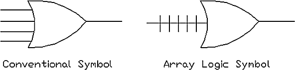
Array Logic Symbols for OR gate
- Instead of having multiple input lines to the gate, a single line can be drawn as shown. ROM is one example of PLD. Other such devices are Programmable Logic Array (PLA), the Complex Programmable Logic Device (CPLD) and the Field Programmable Gate Array (FPGA).
- In digital systems, memory is a collection of cells capable of storing binary information. In addition to these cells, memory contains electronic circuits for storing and retrieving the information.
- There are two types of memories used: Random Access Memory (RAM) and Read Only Memory (ROM). RAM accepts new information for storage to be available later for use. RAM can perform both read and write operations.
- The memory write operation enables us to write data into the memory and read operation allows us to read data from the memory. Unlike RAM, ROM can perform only the memory read operation. This means that in ROM, the information can not be altered by any way, and in RAM the information can be stored inside the memory and can be retrieved any time when required.
Random Access Memory (RAM)
- The cells in a memory can be accessed to transfer information to or from any desired location. In RAM, the information is accessed from the cells and the access time does not depend upon the location of the memory cell. In serial memory, i.e. in magnetic disk or tape unit, it takes different lengths of time depending on the desired location relative to the current physical location of the disc or tape. There are two categories of RAM: Static RAM (SRAM) and Dynamic RAM (DRAM).

Block diagram of a memory
- RAMs comprise a generic category that encompasses all memory devices in which the contents of memory address can be accessed at random. The above figure shows the block diagram of a memory. The n data input lines provide the information to be stored in the memory and n data output lines supply the information coming out of the memory. The k address lines specify the particular word chosen among the many available.
- If a memory has k address lines, then it can have 2K memory locations. The name given for a memory location is known as an ‘address’. It means that a memory with k address lines can store 2K words (or bytes).
- In the DRAM, the storage of information is inherently only temporarily. As a consequence the information must be periodically refreshed. A capacitor is used to store the electrical charge. If there is a sufficient charge on the capacitor, it means that logic ‘1’ is stored. Since the capacitors are not perfect, there can be leakage due to which information is likely to be lost and hence the charge has to be refreshed periodically.
- SRAM does not need to be refreshed. The need for refresh is the primary logic difference in the behavior of SRAM and DRAM. For SRAM, the logic model used for the cell is a Latch or a flip-flop. It consumes more power than DRAM.
Read Only Memory (ROM)
- A Read Only Memory is a device in which permanent binary information is stored. The information must be specified by the designer and is then embedded into the ROM to form the required interconnection or electronic device pattern. Once the pattern is established, it stays within the ROM even when the power is turned off and on again; such that ROM is non-volatile.
- ROM chips contain a grid of columns and rows and use a diode to connect the lines if the value is a 1. If the value is 0, then the lines are not connected at all. They consume less power and are highly reliable.
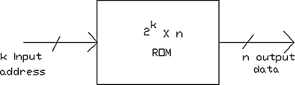
Block diagram of ROM
- In the above block diagram, there are k inputs and n outputs. The inputs provide the address for the memory, and the outputs give the data bits of the stored word that is selected by the address. The k address input lines can specify 2K words. ROM does not have data input because it does not perform a write operation.
- Following are some basic types of ROM:
- Programmable Read Only Memory (PROM)
- Erasable Programmable Read Only Memory (EPROM)
- Electrically Erasable Programmable Read Only Memory (EEPROM)
- Flash Memory
- In a PROM chip, with a grid of columns and rows, there is a fuse at every intersection of columns and rows and the fuse can connect them. The contents of PROM can be erased by flooding the chip with ultraviolet radiations. They are programmed by the user.
- As the name suggests, EPROM can provide the facility of re-writing the chips several times. They are configured using an EPROM programmer that provides voltage at specified levels. For erasing, an ultraviolet light of certain frequency is used.
- The EEPROM is also known as Read Mostly Memories (RMM). The contents of this memory can be altered electrically. It requires some circuit techniques that are not found commonly in normal logic circuitry. Hence it a slow process. In contrast with EPROM, here the complete chip does not have to be erased to change the specific portion of it.
- Flash memory is a type of EEPROM which uses in-circuit wiring to erase by applying an electrical field to the entire chip or predetermined sections of it called blocks. They work faster than EEPROM because it writes data in chunks, usually 512 bytes in size, instead of a byte at a time.
Testing of RAM
- In case of a semiconductor random access memory, many a times, the stored information is lost when the power supply is switched off; i.e. they become volatile. A battery maintained power supply can be used to avoid this problem.
- Usually a RAM which is not in good order gets warm fast. So, the first and easiest test can be touching the surface of the RAM. In order to check address and data lines, a logic probe can be used. The data over the input and output lines of the chip can be checked and observed.
- If these signals are normal, then it possible that the chip is not storing and reproducing the data accurately. This is tested with a diagnostic software program. The software writes a pattern into each memory space in RAM and it verifies those spaces and sees if the correct information is stored. The software gives an indication in case of a problem.
- The problem with a dynamic RAM can be a delayed refresh signal or the refresh signal is absent. So, in the case of DRAM, the line which handles the refresh signal is checked.
Testing of ROM
- As said above, the chip is first checked for data flow and temperature. If these are not the problems, then find out whether the chip is working or not with help of a logic probe. The power supply is checked.
- Like RAM is tested with a diagnostic software program, in the same way ROM can also be tested. The program verifies the data that is supposed to be stored in RAM and compares this with the data from a RAM that is known to be good. If there is any discrepancy, it is located immediately.
5.7 Practical Tips
- The test signals must not be applied when the power is off.
- An IC should never be removed or inserted while power is applied to avoid possible damage due to current surges.
- Power supply voltages should be checked at the actual IC pins, and not between board connections on the PCB.
- In digital circuitry, large test probes should be avoided. These can short out IC pins and cause more faults.
- Probe pins on devices, not pins on sockets.
- Temperature of the components should be checked with the finger to access for shock hazard. Faulty components tend to be hotter than good ones when operating.
5.8 Precautions
- Handle IC packages without touching the pins.
- Do not use tools which generate a static charge.
- Avoid placing tools or electrical parts on insulators, such as books, paper, rubber pads, plastic bags, etc.
- The grounded equipment should have rubber feet or other means of insulation.
- The work surface (bench top) must be conductive and reliably connected to earth ground through a safety resistance of 250 K Ω and 500 M Ω.
- When testing static charge-sensitive devices, DC power should be on before, during and after application of test signals.
- When boards or components (whether hard-wired or plug-in) are removed or inserted, ensure that all voltages are switched off.
- Enclose IC packages or circuit boards in conductive envelopes during transportation.
5.9 Summary
Analog and Digital signals are mathematical representation of a signal, which is useful when some information is required to be processed.
The basic element of all digital circuits are logic gates that perform logical operations (AND, OR etc) on their inputs.
A logic circuit can have three basic signals: Logic 1, Logic 0 and a pulsating voltage signal that alternates between 0 and 1. A logic probe is used to measure these signals. It is always preferred over a voltmeter in digital troubleshooting.
The logic probe detects voltage levels or pulses at a given point in a digital circuit.
A Logic Pulser is used to stimulate digital circuits and supplemented by a logic probe it aids in testing for circuit response to easily check gates, lines, buses and nodes. The Logic Current Tracer detects whether current is flowing or not and where the current is flowing.
A logic comparator clips onto powered TTL or DTL ICs and detects functional failures by comparing the in-circuit test IC with a known good reference IC. The Logic Analyzer includes an oscilloscope for displaying various digital states.
Functional, AC and DC are the tests used for troubleshooting of ICs.
Electronic systems can be sub-divided into smaller sub-systems that are easily recognizable units like oscillators, power supplies, regulators, digital circuits and so forth. The technician must have a fair knowledge of troubleshooting of these sub-systems in order to troubleshoot an electronic system successfully.
Learning objectives
- Study power supply and its functionality
- Understand how to protect and troubleshoot power supply
- Know the best selection of power supply
- Study of regulators
- Study of protection of regulators
- Study of SMPS
- Understand common problems with SMPS and testing
- Study and test Amplifiers and Oscillators
6.1 Power Supply
Introduction
- For testing of circuit boards and individual components, regulated and stabilized power supply is an essential requirement in troubleshooting. The basic power is from AC mains supply.
- The purpose of the power supply is to convert the 230 V, 50 Hz AC mains supply into a form necessary for operating the internal circuitry of the equipment, which is usually a regulated DC voltage.
- Usually different power supplies are required for different circuits but in general the following voltage and current rating power supplies are essential for mixed signal applications:
- Digital circuits: 6V, 5 Amp
- Analog circuits: ± 25V, 1 Amp
- Depending upon load conditions, a power supply can be a constant voltage power supply (stabilizes output voltage) or a constant current power supply (stabilizes output current).
- A typical line connected power supply performs the following functions:
- Voltage Conversion: 230V AC line voltage is converted to one or more other voltages as per the application.
- Rectification: converts AC to DC.
- Filtering: smoothes the rectified voltage.
- Regulation: makes the output voltage independent of line and load variations.
- Isolation: separates the supply outputs from any direct connections.
- Normally, a power unit has more than one output.

Power supply arrangement
- The above figure shows a typical power supply arrangement in electronic equipment. A rectifier (Diode Bridge) is used to convert alternating voltage into uni-directional voltage, which is followed by a filter circuit (a large capacitor) to smooth out the pulsating DC.
- For each output voltage, a separate transformer secondary winding is employed.
- A badly designed power supply can cause problems in functioning and efficiency of a circuit as shown in the following figure. In these figures the characteristics of an audio amplifier are compared with and without a regulated power supply.
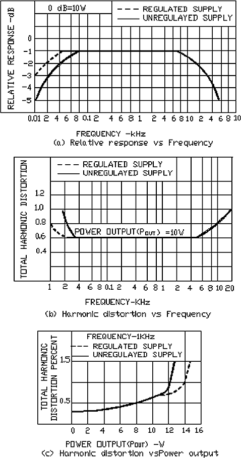
Performance Curves of an Audio Amplifier
Protection Techniques
- Protection in a power supply is important for the power supply itself and for the load. High line voltages, excessive load demands, line or load generated transients, inordinate temperature rise, etc. are the conditions which can damage a good power supply and hence the protection is required.
- The series pass transistor is the most important component for protection against the above said conditions. Many circuits make use of a fuse. But this fuse is not sufficient to protect semiconductors. A current limiting circuit is widely used. When there is a large heat dissipation in the circuit which gives rise to a prolonged over current, a simple current limiting circuit is not sufficient. A ‘crowbar’ or ‘fold back’ circuit gives better protection.
- To protect a power supply, two clamping diodes can be connected across the input of the comparator. A zener diode or a neon lamp can be used to limit the drop across the series pass transistor. An RC network is employed to attenuate incoming transients from power lines.
- There is a possibility of transients in a power line, which can badly damage discrete semiconductors and ICs. The transients include mysterious spikes. These spikes can develop in switching on or off a power supply which may damage the unit.
- To overcome this problem some energy absorbing devices can be connected across the power line or across the secondary of the power transformer. These devices include zener diode, silicon carbide (thyrites), neon lamp, RC network, and energy absorbing devices
- EMI and RFI are the factors which can cause deviation in the power supply. To protect power supply against these interferences, EMI filters, shields or Ferrite beads can be employed. Proper grounding also reduces these effects. Power supplies with isolation and decoupling units are considered to be effective in filtering the conducted interference.
Power Supply Troubleshooting
In troubleshooting power supplies, the following steps are performed:
- Shut off the equipment.
- Disconnect each of the power supply branches from the circuit. This is done to determine whether the problem is in the circuit or in the power supply itself.
- Now turn on the power supply and check. If the power supply returns to normal, the circuit fed by the power supply is to be examined. The problems could be a faulty IC or a short circuit in printed circuit traces. Carefully inspect the circuit board for obvious problems. If it is broken connections, then look for a solder bridge or cracked circuit foil. However if there is still a problem, it means that the power supply itself is bad.
- For a bad power supply, the problem is most likely caused by a faulty transistor, IC or a diode. The component is probably shorted.
- As said earlier, a capacitor is used to filter out AC and give a smooth DC output voltage. If this capacitor fails, some excessive AC will be present as ripple, which gives rise to faults: The presence of ripple is checked with an oscilloscope. Check for a smooth and clear output at each power supply branch. If the ripple is found to be present, the filter capacitor is to be checked.
In some cases, excessive ripple is also observed if the regulating circuit is faulty.
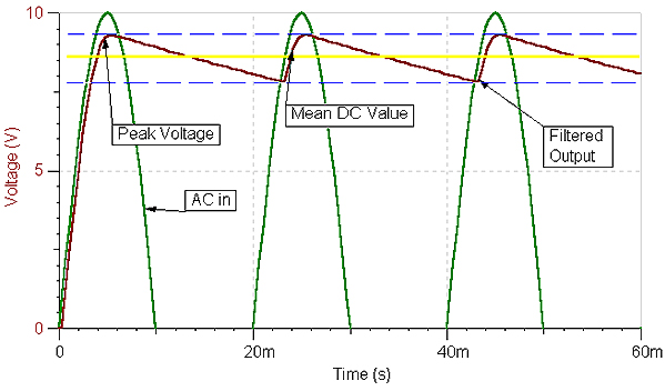
Presence of ripple
- Sometimes, a power supply may be found to give high or low output voltage. To correct this voltage some circuits provide some adjustment. This includes a ‘trimmer pot’ with a screw driver. The voltage is controlled by turning this trimmer pot as per the requirement. However, voltage IC regulators do not need such a type of adjustment provision.
Selection of Power Supply
For the selection of power supply the following questions must be answered:
What is the voltage range over which the system must perform?
How much current does the system require?
How much ripple voltage can be tolerated?
How much voltage drift with temperature is acceptable?
Do we use one larger regulator or many individual regulators, to match the various load impedances?
Which type of regulator is most suited?
Having answered all the above questions, one can select a perfect power supply. However, cost and size of the power supply and consequently the system is equally important from the selection point of view.
Practical Tips
- The power supply is connected to the AC mains by a cable and a plug. Ensure that all the three wires are intact and connected to the respective pins in the plug.
- A fuse can be used to protect the power supply. The fuse is usually placed at the back of the equipment enclosed in a black cap. If the equipment is not working, disconnect it from the mains supply, unscrew this cap and check the fuse with VOM.
- Check the presence of the mains voltage in the socket to which the equipment is intended to be connected.
6.2 Regulators
Introduction
- Most electronic circuits require a direct voltage supply that is usually derived from AC supply by transformation, rectification and filtering. The resultant raw DC is not sufficiently stable for most purposes. It normally contains an unacceptably large AC ripple waveform.
- To render the voltage more constant and to attenuate the ripple, voltage regulator circuits are employed. All voltage regulators must have a stable voltage source which is provided by a special kind of diode (breakdown or zener diode).
- A breakdown diode with a series connected resistor can operate as a simple low-current voltage regulator. A regulator performance is further improved by the addition of an error amplifier to detect and amplify the difference between the output voltage and the voltage reference source.
- Complete voltage regulator circuits are available in IC form. Some IC regulators are simply connected to a supply to provide a fixed output voltage.
- In many cases, instead of controlling power supply voltage, it is possible to control the current using a feedback circuit and current regulator. In some cases, both current regulator and voltage regulator are used in the same circuit.
Types of Regulators
Depending upon the technique which is used to provide regulated DC voltage, regulators are divided into the following three types:
- Linear Regulator
- IC regulators
- Switched Mode Power Supply
Linear Regulators
- This is the most widely used type of supply. It is a high gain control circuit that continuously monitors the DC output voltage and corrects the output so that it almost remains constant irrespective of the changes in the load current and input AC voltage.
- The following figure shows a discrete voltage regulator:

Discrete Voltage Regulator
- Transistor Q2 is the emitter follower. It is a pass transistor as all the load current passes through it. A voltage divider circuit R1 and R2 samples the output voltage Vout and delivers a feedback signal Vf to the base of transistor Q1. Q1 acts as a linear amplifier. The input to the regulator is from an unregulated power supply consisting of a power transformer, rectifier and a capacitor input filter.
- Typically Vin has a ripple of 10 percent of the DC voltage. The output of the regulator is practically free of any ripple. Since the feedback is used, any changes in the open loop gain, load resistance and line voltage is automatically compensated.
Protection of Linear Regulators
Several features need to be incorporated in the series regulator circuits to protect them from overload currents. The two schemes that are usually employed for this purpose are discussed below.
Fold back Current Limiting:
This makes the power supply switch, to give almost zero output voltage if the value of the load current is exceeded beyond its specified range:
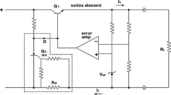
Fold back current limiting circuit
An SCR is the device which is used to limit the current.
A current monitoring resistor is placed in the power supply return line.
The voltage developed across this resistor is used to switch on SCR.
In case of an overload, SCR is switched on and the voltage across it falls to approximately 0.9V, which is insufficient to forward bias the series transistor.
The result of this is an appearance of zero voltage across the output.
If SCR is triggered once, it remains on until the fault is removed, after switching off the power supply, the output will remain zero.
Over Voltage Protection
Over voltage protection is required for all the digital circuits. If their Vcc terminal receives more voltage than required, then the ICs get damaged.
A zener diode is used to achieve the over voltage protection:
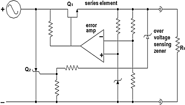
Over voltage protection circuit
The zener senses the voltage across the power supply’s output terminal.
When the DC voltage rises, the zener starts conducting. This turns on SCR Q2.
The voltage at Q1 collector falls rapidly to zero and the fuse blows.
Above circuit can be called as Crowbar Circuit, which limits the output to the pre-set value.
IC Regulators
- IC regulators are used in most of the modern power supplies. µA 723 is the most common IC regulator with 10 lids and 14-pin DIP encapsulation:
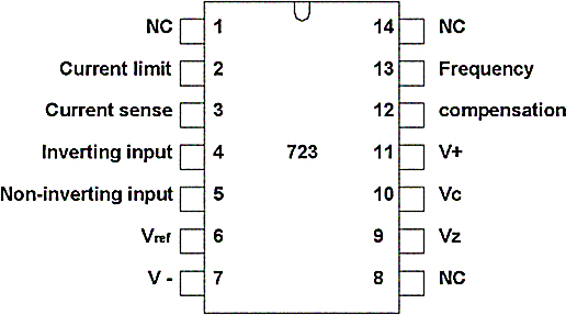
µA 723- pin configuration
- This IC contains internally, a reference source, error amplifier, series transistor, and a current limiting resistor.
- For this IC, the input voltage must be at least 3V higher than the expected output voltage and a low value capacitor must be present between the frequency compensation pin to inverting input to avoid oscillations at high frequencies.
- Today ICs are available with only 3 terminals, one for unregulated input, one for regulated output and one for the ground:
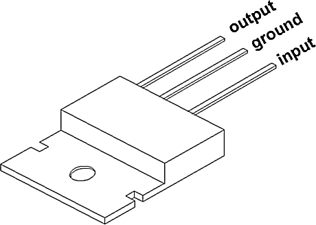
Three terminal IC regulators
- In 3-pin voltage regulators the input is applied between the centre leg and the input terminal. The output is measured between the centre leg and output terminal.
Testing Voltage Regulators
- Using a multi-meter, troubleshooting of voltage regulators can be performed. For example testing of 3-pin voltage regulator is shown in the following figure:
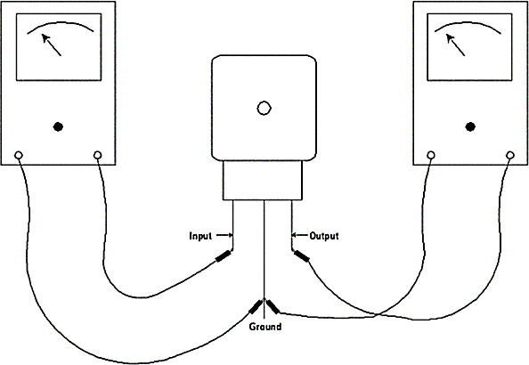
Testing 3-pin Voltage Regulators
- With the equipment turned on, check the input voltage to the regulator. It should be at least one volt higher than the specified output voltage.
- Check the output voltage, which should be nearly equal to the specified output voltage.
- If the input is present, but the output voltage is not correct, check for ground connection of the centre leg of the regulator.
- In case of overload or short circuit, the regulator cuts off the output. To check this condition, the output of the regulator is disconnected from the circuit to be driven and the output voltage is measured. If the output still does not return to the normal value, the regulator is faulty and should be replaced.
6.3 Switched Mode Power Supplies (SMPS)
- It is also known as switching power supply or sometimes chopper controlled power supply. By using a switch as a series element and controlling the on and of time we can vary the average voltage at the DC output level.
- It uses high frequency switching devices such as BJT, MOSFET, and thyristor to take directly rectified line voltage and convert it to a pulsed waveform:
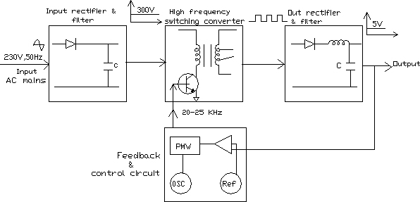
Functional Block diagram
- The above figure shows four major blocks of SMPS:
- Input rectifier and filter
- High frequency inverter
- Output rectifier and filter
- Feedback and control circuit
- The AC mains is rectified and filtered. The high voltage DC is then fed to the high frequency inverter. The operating frequency range is from 20 KHz to 1 MHz.
- The high frequency square wave thus generated is stepped down by the high frequency transformer and then rectified and filtered to produce the required DC output.
- The output is compared with a reference and pulse width modulated to get the desired regulation by the control circuit. The regulation of the output voltage is achieved by varying the duty cycle of the square wave.
- When the load is removed or input increases, the slight rise in the output voltage will signal the control circuit to deliver shorter pulses to the inverter. Conversely, as the load is increased or input is decreased, wider pulses are fed to the inverter.
- The efficiency of an SMPS is higher than a series type regulator. They are physically smaller and lighter than linear regulators.
- They are noisy electrically and sometimes audibly. Thus they are unsuitable for powering circuits that are sensitive to electrical noise unless adequate filtering and shielding is provided.
Common Problems with SMPS
- The switch mode power transistor or other semiconductor devices can be shorted which can cause the supply to be dead.
- The output goes out of tolerance if the main filter capacitor is dried up or leaky. It may also give excessive ripple at the line frequency.
- In these supplies the components are usually large ones. So there is always a possibility of bad solder connections.
- The actual cause of failure may be power surge, burn-out, lightening strikes, random failure, or primary side electrolytic capacitor open or with reduced capacity.
Testing SMPS
- When testing SMPS, each branch of the supply will shut itself off, if its load is disconnected. For this reason, a load resistor must be connected to each branch during testing.
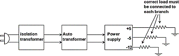
Testing SMPS
- The value of the load resistor to be connected would depend upon the current rating of the supply. An isolation transformer and an auto transformer are connected in the AC line during the test. The auto transformer is useful for varying the AC voltage and the isolation transformer is useful for protection.
- If this equipment are not available, the troubleshooting of SMPS should be limited to visual inspection for burnt or damaged parts.
6.4 Oscillators
Introduction
- Oscillators are used to generate periodic waveforms without any input signal. If the loop gain and phase is correct, then oscillators produce an output which is in the form of oscillations.
- A sinusoidal oscillator needs an amplifier and a phase-shifting network. The amplifier receives the output of phase shifting network, amplifies it, phase shifts it through 180 degrees and applies it to the input of the network. The network phase shifts the amplifier output through another 180 degrees and attenuates it before applying it back to the amplifier input.
- When the amplifier gain equals the inverse of the network attenuation, and the amplifier phase shift equals the network phase shift, the circuit is amplifying an input signal to produce an output which is attenuated to become an input signal. The circuit is generating its own input, and a state of oscillation exists.
- There are many types of oscillator circuits like Colpitt’s oscillator, Hartley oscillator, Wein Bridge oscillator, phase shift oscillator, etc, each with its own limits and advantages. There are transistor oscillators also which are used in television time bases, tape recorder oscillators and so on.
- Crystals are widely used in oscillators because of their inherent stability. In crystal oscillators, the tendency to drift which limits the usability of oscillator is very low. In tuned oscillator, the oscillator frequency can be tuned to certain kilohertz.
- For oscillations to be sustained, Barkhausen criteria must be satisfied. The criteria is that the loop gain of the circuit must be equal to (or greater than) 1 (one), and the phase shift around the circuit must be zero.
Faults and Causes
- The major fault can be a lack of oscillations, which can happen because of faulty transistor, incorrect dc conditions, inadequate loop gain, and open signal bypass.
- The oscillator may produce low output, the cause of which can be low loop gain, low value charging C or high value R (blocking capacitor).
- The frequency of the oscillations can be incorrect. This can be because the LC circuit goes out of tune. RC component values should be correctly maintained.
- Frequency drift and distortion are also the major faults, the reason being, temperature change, component aging, transistor bottoming.
Troubleshooting
Following are the troubleshooting techniques against High frequency oscillations, Low frequency oscillations, Ground loops and supply bypassing.
High frequency oscillations
- This is caused by magnetic or capacitive coupling between the input and output stages. Refer to the following figure (a).
- In a typical amplifier the output stage and the input stage will form the two plates of a capacitor and this can give a feedback path at high frequencies. The wires of the output and the input stages can become the primary or secondary of a transformer respectively producing a feedback effect:
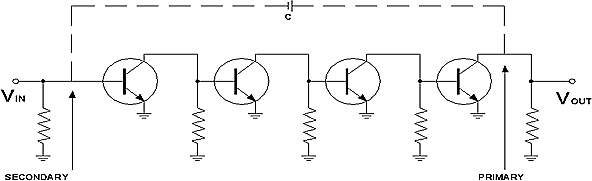
(a) Capacitive and Magnetic coupling from output to input
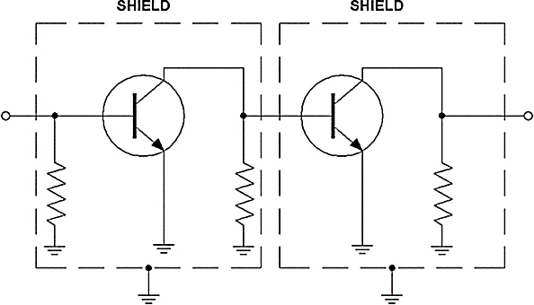
(b) Shields enclose each stage and prevent oscillation

(c) Baffle shield prevents capacitive coupling
- Proper layout of the stage with a metallic shield for each stage can avoid these problems. Refer figure (b). If only capacitive coupling is the problem, then a metallic ‘baffle’ plate can be used between the stages. Refer figure (c).
Low frequency oscillations
- The cause for this can be the non zero impedance of the power supply. An ideal power supply should have zero impedance. Finite impedance will lead to current feedback from the output stage to input stage.
- The solution for this is to use a regulated power supply with internal impedance of 0.1 ohm.
Ground Loops
- Ground loop means difference in potential between various ground points in equipment:
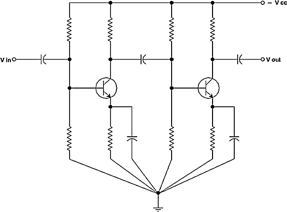
Single ground point prevents ground loops
- Actually whenever the chassis serves as a ground which has come as non-zero impedance then the ac ground current of the last stage may happen to flow through that part of the chassis being used by another stage.
- In order to avoid this problem, a single ground point is provided as shown in above figure.
Supply Bypassing
- A long lead between the power supply and the circuit can have enough inductance to cause a feedback effect especially at high frequencies:
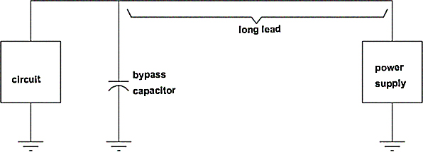
Supply Bypassing
- The solution is to have a large bypass capacitance near the circuit. This is essential for digital ICs. The bypass capacitor must be as close to the IC as possible.
- The bypass capacitor prevents current feedback caused by a long lead between power supply and circuit.
6.5 Amplifiers
Introduction
- Some basic amplifying devices are Bipolar Transistor, triode, JFET, MOSFET, etc.
- A power amplifier or a large signal amplifier develops large output voltage across low impedance loads. Audio amplifiers are large signal amplifiers which supplies ac output power to low impedance speakers.
- Power amplifiers may be categorized as class A or as class B or class AB push pull amplifier.
- The amplifier load may be transformer-coupled, capacitor coupled or direct-coupled. Direct coupling usually gives best performance, but positive and negative supply voltages are required.
- In output stage, power MOSFET can be used instead of bipolar power transistors to get better performance.
Testing Amplifiers
- There are several basic measurements that are useful to check whether most amplifiers are in working order.
- Amplifier Voltmeter Test is one which can be used.
- In class A amplifier, the collector (or drain or plate) voltage should be about one half of the power supply voltage. Therefore, after measuring the power supply, the next voltage measurement is at the collector output. That will tell you if the amplifier is working and if it is conducting an amount typical of a class A amplifier.
- If the voltage is too high it means that the amplifying device is not conducting enough current. If the voltage is too low it means the transistor is conducting too much current. This can be because of a bias problem or a defective transistor.
- Once the faulty stage is located, further tests can be performed to determine which component is at fault. You may also determine the condition of an amplifier by measuring amplitude of the AC input and the AC output signal with an oscilloscope. Most voltage amplifiers should show a certain amount of gain. That is, the output AC voltage should be more than the input. That is not true of power amplifiers, or emitter follower amplifiers.
- An AC voltmeter can be used for that tests but you must know the frequency limit of your meter. Usually, a voltmeter can be used at all audio frequencies. If the voltmeter is sensitive enough to measure the input signal strength, in that case a Prescaler can be used. That is an amplifier with a specific voltage gain. It amplifies the weak input signal so it can be measured with a voltmeter:
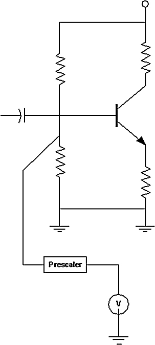
Prescaler
- As shown in the above figure, you have to divide the measurement by the voltage gain of a prescaler
- In a Power amplifier it is quite common that the amplifier is working very well but the output voltage is not as high as input voltage. That is typical because the output of a power amplifier should be a signal current. Where that current flows through a low value of load resistance, such as in a speaker, the voltage gain may be relatively low even though the power gain is high.
- The kind of amplifier should be known when making an AC input/output voltmeter test.
- A Short Circuit Voltmeter Test is used for bipolar transistor amplifiers. This test determines if the bipolar transistor is not only passing the current but also that it has control over that current.
- If in a particular case the collector voltage is half of the supply voltage, it can be due to the fact that there is an emitter collector short circuit inside the transistor. The transistor is faulty even though the collector voltage measurement is correct:

Short Circuit Voltmeter Test
- As shown in the figure, the transistor will be turned OFF by shorting the emitter to the base. The collector voltage should go high and in fact, it should be almost equal to the power supply voltage.
Practical Tips
- Power transistors are usually large (physically) compared to voltage amplifiers.
- Power transistors operate at higher temperatures. They are often mounted on heat sinks or metal chassis.
- Do not use Short Circuit Voltmeter Test for amplifiers that use FET or tube amplifying devices.
- Short Circuit Voltmeter Test is useless for class B amplifier. These amplifiers are biased at cutoff and will not conduct unless there is an input signal. Since the amplifier is already at cutoff the short circuit will not produce any change in the DC output voltage.
6.6 Troubleshooting of RS-232C Serial Data Standard
Introduction
- RS-232C is defined in reference to DTE and DCE i.e. Data Terminal Equipment and Data Communication Equipment. The devices which are used to send the data are known as Data Communication Equipment (DCE). The terminals or computers that are sending or receiving the data are referred to as Data Terminal Equipment (DTE).
- In response to the need of signal and handshake standards between DTE and DCE, the RS-232C standard is developed. The rate of data transmission in RS-232C is restricted to a maximum of 20kbaud with a distance not more than 50feet.
- It specifies 25 signals, which are divided into four groups: data signals, control signals, timing signals and ground. The voltage levels are not compatible with TTL logic levels. For data lines, the voltage level +3V to +15V is defined as logic ‘0’; from -3V to -15V is defined as logic ‘1’ (normally voltage levels are ± 12V). This is a negative true logic. However other signals are compatible with the TTL level. The following figure shows the 25 pins and signals of RS-232.
- Out of the 25 pins of the connector, there are some pins that are not used for data transmission. These pins are mainly used for the loop-back testing of the port.
- RS-232 protocol identifies how fast data is transmitted between two ports. This transmission speed is defined as Baud Rate which is roughly equivalent to the number of bits transmitted per second. As mentioned above, the baud rate will vary from 1200 to 19200. Common baud rates are120, 1400, 4800, 9600 and 19200.
- The length on the interconnecting cable between a control system (computer) and controlled equipment must decrease as the bud rate increases. At 9600 baud rate, the cable length can be 50 feet to the maximum and at 19200 baud rate; the cable length should not exceed 20 feet:
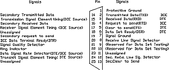
RS-232C: Pins and signals
- Because of the incompatibility of the data lines with TTL logic, voltage translators called Line drivers and Line receivers are required to interface TTL logic with RS-232C signals. An example of RS-232 is its use in Interactive Voice Response System. In IVRS, it is used as a serial interface standard, which transmits the data serially. The interface is used between the microcontroller and PC.
Common Problems with RS-232C
- No information is transferred
- Unable to communicate with the machine to which it is connected
- Any garbled information is transferred
- Only sends or receives files and unable to perform both
- Only a part of a file is transmitted
- Interruption in transmission
Troubleshooting of RS-232C
Many a times the problem occurs when connecting a control system to a device. A control system can be a PC and a controlled device can be any RS-232 based controlled device for example a telephone modem. The reason can be improper wire connection. When the connection of a control system to the controlled device is being done, the Transmit and Ground pins of the control system are connected to Receive and Ground pins on the controlled device respectively:
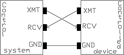
Connection of control system to a controlled device
In the above figure, the short forms are used as follows:
XMT —– Transmit pin,
RCV —– Receive pins, and
GND —– Ground pins
The XMT pin from controlled device is connected to RCV pin of control system. This is done because the control system can receive an acknowledgement from the controlled device after the completion of data transfer.
Unless all the pins are labeled, it is difficult to make the proper wiring between the control system port and controlled device port. If the controlled device uses a terminal block type connector, it is quite easy to test the voltage using a voltmeter to ensure that the connection has been made correctly. The following figure shows the incorrect connection. Here the Receive and Transmit lines are reversed:

Incorrect connection
Set the voltmeter to ‘DC’, and test the voltage between the RCV and the XMT pin. The voltage on the Receive line stays at 0V, and the voltage on the Transmit line can be any value between -6V to -12V.
In order to ensure the correct interconnections, as shown below, test the voltage between the RCV pin and GND pin on the terminal block connector. The reading should be between -6V to -12V. The XMT line should also show the same reading:
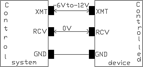
Correct connection
Even after overcoming the problems due to wrong hardware connections, the problems appear, then you should confirm the communications software properties settings for both the control system and controlled device. The baud rate of both the devices should be identical. If the baud rate of the control system is 4800, the same should be the baud rate of the controlled device.
Data bit, stop bit and parity bit should also be defined properly. The data bit indicates how many bits are there in a single character to be transmitted; the parity bit defines the number of 1s during one byte transfer as even or odd; the stop defines the end of the data to be transmitted. Standard settings for these parameters for most A/V devices are 8, none, and 1 respectively.
6.7 Troubleshooting Microprocessor based Systems
Introduction:
Microprocessor is a clock driven semiconductor device consisting of electronic logic circuits. It is capable of performing various computing functions and making decisions. It is also known as a CPU (Central Processing Unit) that is fabricated on a single chip. All the logic circuitry, control units are fabricated on a single chip which is a thin piece of silicon onto which transistors making up the microprocessor have been itched.
A microprocessor is divided into three major parts:
- ALU (Arithmetic Logic Unit)
- Register Array
- Control Unit
ALU (Arithmetic Logic Unit)
Using a ALU microprocessor can perform mathematical operations like addition subtraction, multiplication and division. It also performs logical operations like AND, OR, EX-OR, etc.
Register Array
The register array consists of various registers like B, C, D, E, H, L. The registers are primarily used to store data temporarily during the execution of a program. The user can access the registers for temporary data storage and transfer.
Control Unit
The control unit provides the necessary timing and control signals to all the operations in a microcomputer. It controls the flow of data between microprocessors and memory and peripherals.
- In a microprocessor based system, the microprocessor provides special codes for getting the information into and out of the memory, operates on coded information and delivers the result to some output destination.
- A microprocessor, in which most of its instructions operate on n-bit data, is called as an n-bit microprocessor. 8085 is 8-bit microprocessor because most of its instructions operate on data which is 8-bit wide. So an n-bit microprocessor has n data lines on the data bus:
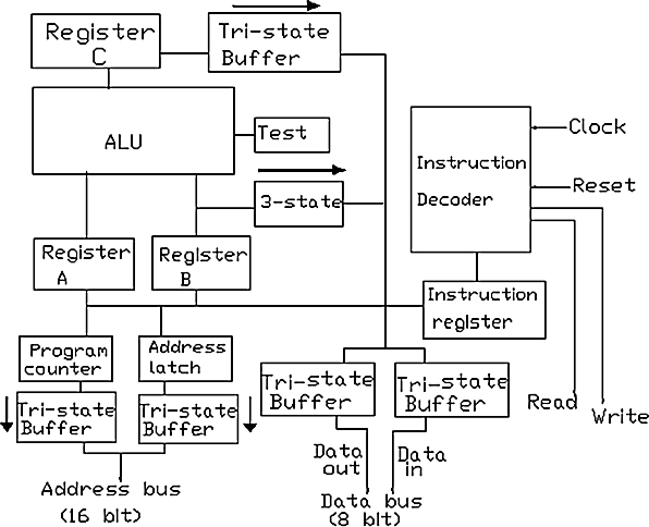
Block Diagram of a Microprocessor
The microprocessor has:
- An address bus that may be 8-, 16-, or 32-bits wide which sends an address to memory
- A data bus that may be 8-, 16-, or 32-bits wide that can send data to memory or receive data from memory
- An RD (read) or WR (write) to tell the memory whether it wants to set or get the address location
- A clock line that lets a clock pulse sequence the processor; and
- A re-set line that resets the program counter to zero (or whatever) and restarts the execution
In the above block diagram of microprocessor registers A, B and C are simply latches made out of flip-flops.
The program counter is a latch used to hold memory address of the next instruction to be executed. It is incremented by 1, or reset to zero when given proper instruction. It keeps the track of memory address of the instruction in a program during the execution of instruction.
The instruction register and instruction decoder are special purpose registers which are responsible for controlling all the other components.
The tri-state buffers can pass a 1, a 0 or it can disconnect its output. It allows multiple outputs to connect to a wire, but only one of them to actually drive a 1 or a 0 onto the line.
The ALU performs all arithmetic and logical operations as said above. The Test register attached to ALU holds some values and can compare two numbers. The instruction decoder uses the value stored by the test register to make a decision.
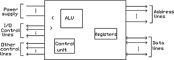
Inside and Outside of a Microprocessor
As said earlier, the microprocessor is divided internally into three major parts: ALU (Arithmetic Logic Unit), Register Array, Control Unit. It is shown in the above figure. The microprocessor has the following sets of lines attached to it:
- Address Lines
- Data Lines
- Control Lines
Address Lines
The microprocessor has several address lines over which it transmits an address to the off-chip memory or to the I/O devices. Collectively they are known as Address Bus. A typical 8-bit microprocessor would have an address bus of 16-bits to transmit the address, for example the address is 16-bits wide. So the microprocessor can access to 216 means 65,536 memory locations.
Data Lines
Data Lines are a set of lines to transmit and receive data. Collectively they are known as Data Bus. A typical 8-bit microprocessor would have 8-bits data bus (for example 8085); a 16-bit microprocessor has 16-bits data bus (for example 8086).
Control Lines
These are the lines to control the signals from input and output devices. The devices could be an electric motor, seven segment display, etc. They also generate control signals for input and output devices.
Multiplexing is a useful technique employed with microprocessors for obtaining additional address and data lines. By multiplexing it is possible to handle 16-bit data signals, through an 8-line data bus.
The address and data lines are also multiplexed and we have address and data available on the same physical lines at the different instants of time.
Testing Microprocessors
In a microprocessor based system, if the microprocessor fails to operate as per the requirement, the signals that should be first tested are clock signal, reset signal, address and data lines.
Clock Signal
The clock signal is tested first, because it is one of the inputs to the microprocessor. If the clock signal is at fault, the whole working of the system may break down. It may stop working or may show intermittent behavior. The clock pulse is tested with a logic probe or oscilloscope. In modern CPUs the clock generator is built within the chip and it only requires an external crystal. The working of the crystal and the capacitor in the clock circuitry is also checked.
Reset Signal
The reset signal makes the microprocessor go back to a known starting point. When the reset key is pressed, the pin should go low and then return to high. A logic probe can be used to check the presence or absence of a reset signal. At the key, if an absence of signal is noticed, then the reset signal line is checked.
Address and Data lines
The problem which can occur with address and data lines can be a short circuit with one of the data or address lines on the printed circuit board. The lines can be shortened to power supply (+5V DC), or it can be shortened to ground. Again a logic probe is used to check these lines. Each line should show activity which should be observed carefully whether it shows a steady high or steady low indicating a short to power or ground respectively.
The address and data lines are associated with tri-state buffers. If there is any failure in any one of these buffers, the correct signal will not reach the CPU.
If the suspected faulty line does not show short or break and tri-state buffers are also working fine, then there is a possibility of a problem in the other ICs associated with the line.
Troubleshooting of Microprocessor based System
- As noted above, a microprocessor based system has a CPU, memory and I/O section. The microprocessor operates on instructions, i.e. software. It means that the failure of a microprocessor based system can be due to hardware or a software problem.
- The first step for troubleshooting of a microprocessor based system is to understand what the problem is. This involves the knowledge of control signals produced by a microprocessor. The maintenance technician should know the functions of peripheral devices.
- Logic clip, logic probe, logic pulser, current tracer, logic analyzer are the troubleshooting tools which can be used to solve hardware problems.
- Many a times the problem comes in the power supply section. The malfunctioning of the power supply may cause failure of discrete components like diodes, transistors, resistors and capacitors.
- The peripheral devices are connected to the microprocessor with the help of digital ICs which fail more often as compared to discrete components. These devices heat up when the system is on and cool down when the system turns off. This hot-cold-hot effect can cause a break in the connection of a wire leading from inside the chip to a pin, producing an open circuit. In this case, the chip becomes unpredictable and the output can be stuck at 1 or stuck at 0.
- There can be electrical transient noise which comes from voltage spikes from power lines. They can cause a program and generate incorrect data which can change program counter data. Unpredictable change in program counter may crash the whole program.
6.8 Summary
The purpose of the power supply is to convert the 230 V, 50 Hz AC mains supply into a form necessary for operating the internal circuitry of the equipment, which is usually a regulated DC voltage.
Voltage conversion, rectification, filtering, regulation and isolation are the main functions of power supply.
For a bad power supply, the problem is most likely caused by a faulty transistor, IC or a diode. The component is probably shorted.
Voltage regulator circuits are employed, to render the voltage more constant and to attenuate the ripple. Voltage regulator circuits are also available in IC form which is very popular.
Linear Regulator, IC regulators, Switched Mode Power Supply are the three types of voltage regulator.
Oscillators are used to generate periodic waveforms without any input signal. Lack of oscillations is the major fault in the oscillator which can be because of a faulty transistor, incorrect dc conditions, inadequate loop gain, and open signal bypass.
This chapter gives an idea of how temperature affects an electronic system and what should be the preventive steps to avoid the malfunctioning of the system due to temperature variations. Slightly deviating from the topic, the chapter also provides an understanding of Signal Injection and Signal tracing methods which are used often in troubleshooting processes.
Learning objectives
- Study the effect of temperature on electronic systems
- Study of compensation methods against temperature effects
- Know thermal protection devices for troubleshooting of temperature variations in electronic systems
- Understand Signal Injection with an example
- Understand Signal Tracing with an example
7.1 Effect of Temperature on EC
- Temperature is a parameter which should not be neglected at the time of troubleshooting. It is a factor which plays an important role in maintenance of electronic circuits.
- The components in electronic circuits have some specific temperature requirement which should be met at the time of construction as well as operation of electronic circuits. Otherwise, desired results are hard to achieve.
- At higher temperatures, the expansion of materials and acceleration of chemical changes take place. It is estimated that a failure rate doubles with every 10 degree rise in temperature.
- At low temperatures, some materials may harden and transistor gains may drop. If there is rapid temperature cycling, then continuous expansion and contraction may lead to accelerated failure rate.
- Hence it is advised to refer to the manual to advise oneself about the temperature conditions of the equipment.
- Transistors are badly affected because of the changes in temperature. Hence it is advised to protect the transistor in electronic circuits against temperature effects. Therefore in order to save an electronic circuit, one should always think to save the transistor against temperature.
- Thermister compensation and Sensistor compensation are effective compensation techniques to protect the transistor thermally.
Thermister compensation against temperature effects
- A thermister is a device with a negative temperature coefficient, i.e., its resistance decreases with the rise in temperature. The following figure shows a circuit with thermister compensation:
Thermister compensation
- As the temperature increases, value of resistance Rt decreases, and the current in the thermister increases. This leads to an increase in the current in resistance Re. This increase in current results in an increase in voltage Ve across Re, which increases I2, which in turn reduces the base current Ib. The reduction in base current Ib reduces collector current Ic, thereby compensating for any increase in collector current due to a rise in temperature.
- Alternatively, the thermister can be placed across R2 as shown in the following figure:
Alternate thermister compensation circuit
- When temperature increases, resistance of the thermister decreases, and the value of parallel combination of R1 and R2 also decreases. This leads to an increase in I2 and a decrease in Ib. This results in a decrease in Ic to compensate for any increase in Ic due to a rise in temperature.
Sensistor compensation against temperature effects
- A sensistor is a device with a positive temperature coefficient, i.e. its resistance increases with temperature. The following figure shows a circuit with sensister compensation:
Circuit with sensister compensation
- As the temperature increases, value of RC increases and hence value of parallel combination of R1 and RC increases leading to a decrease in I1. Thus Ib decreases resulting in a decrease in IC to compensate for any increase in IC due to a rise in temperature.
- Alternatively, the sensistor can be placed either parallel to Re or in place of Re as shown in Figure 7.4:
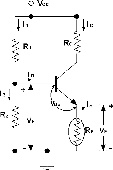
Alternate sensister compensation
- Any increase in temperature results in an increase in Rs resulting in a higher voltage drop Ve. This increases the voltage at the base, leading to an increase in I2 which reduces Ib. A decrease in Ib results in a decrease in Ic, compensating for any increase in Ic due to temperature.
7.2 Testing
- In any electronic equipment, when it is observed that problems come and go by applying and removing heat to a whole area, the heating effect has to be compensated by a cooling effect.
- A circuit coolant (pressurized can) or a coolant spray for different components when the circuit board gets hot. When the defective component is cooled, the trouble can be traced easily.
- The coolant should be used in brief and it should be closely confined to the suspected faulty component.
- The faulty ICs often feel warm or hot. You can use your finger to make a quick ‘touch test’ to find the faulty IC.
Touch Test
- It is recommended to use the back of your finger to make the test as shown in the above figure. The back side of the finger is more sensitive than the tip of the finger.
- A digital thermometer can also be used to measure the temperature of a suspect component.
- Some components are hot even when they are operating normally. If a transistor has a large heat sink, you can expect it to be hot. Take care that you do not touch any part to test temperature which is connected to the mains supply.
7.3 Actual Troubleshooting
There are some devices, which, when used in the equipment, protect the equipment against excessive temperature due to either a fault in the device or improper use of the equipment. These devices are Thermal Protection Devices. Thermal Fuse and Thermal Switch are used widely for temperature protection.
Thermal Protection Devices
Thermal Fuse
- The basic purpose of the Thermal Fuse is to break the circuit at a specific temperature. These are often used in heating appliances. Like electrical fuses, these are one-time only parts.
- In case of failure of this fuse, it can be replaced with another one which meets the electrical and thermal rating of the device. When replacing a fuse, avoid soldering if possible. If at all you need to solder, use a good heat sink on the leads between the thermal fuse and the soldering iron.
Thermal Switch
- Thermal switches come in two types: Strip Type and Disk Type. A typical thermal switch is a small cylindrical device with a pair of terminals and a flange which is screwed to the surface whose temperature is to be monitored.
- In strip type thermal switch, there is a strip of bimetal used, which is similar to thermostat. If there is a change in temperature, it will cause this strip to bend and control a set of contacts. Usually, it breaks the circuit if the set temperature is exceeded.
- Strip type thermal switches are used in appliances with a fixed selection of temperature. They are also used for backup protection in addition to adjustable thermostat.
- The second type is disc type thermal switch. They use a disc of bimetal rather than a strip. This disc is slightly concave in shape. When a set temperature is crossed, the disc pops to the opposite shape. Because of this a set of contacts is activated which breaks the circuit when the temperature is exceeded.
7.4 Signal Injection
The methods of Signal Injection and Signal Tracing are especially useful for troubleshooting systems that have no output. However the methods can be used in all electronic systems.
What is Signal Injection?
- Most of the time system troubleshooting is done by starting at one end and working towards the other. But you can save time by starting in the middle of the system. In such a case, you can divide the system in half and reduce the time for troubleshooting.
- When you are starting in the middle of the system, usually a signal is injected in the system. There is a simple device called signal injector which injects a pulse or a wave (square) into the system being tested. In case of a pulse, its high harmonic contents make it useful over a wide range of frequencies. Signal Injectors can be used in RF, IF and audio stages because of their broad harmonic content.
- In many types of equipment we can inject a test signal of suitable frequency into the input of the equipment and utilize the inbuilt detector or indicator to test its presence at output. Should the applied test signal fail to be indicated in this way and if we are sure that the indicator is OK then we will be pretty sure that the failure is somewhere in the stage or stages between the point of injection of the test signal and the indicator.
- Some technicians use the blade of a screw driver for signal injection when they are working away from their work bench instruments. Using a screw driver blade needs a certain amount of skill and experience. For example, if you tap the center tap of the volume control of a speaker with a screw driver, then the volume control is set for high volume after performing this test.
- Consider the following figure in which signal injection is used to locate a defective amplifier in a dead system:

Signal Injection
- The idea behind this method of testing is to inject a signal into each amplifier one at a time, and then observe the output of the system. If you start by injecting the signal at 1, then 2, then 3, and so forth, you will not get an output signal until you have gone past the trouble. So, if you inject the signal at 2 and do not get the output, but inject at 3 and do get the output, the trouble must be before 3.
- There is an advantage of injecting the signal in the sequence described above. Each time you move the signal source, the output signal will get weaker unless you increase the strength of the signal from the signal generator.
- This is better than starting at the output and moving back. Moving the other way requires a relatively strong signal to be injected at the output. When moving back to the previous amplifier, you can overdrive it enough to cause damage.
Signal Injection with the amplifier signal
- In the above figure, if you have a reason to suspect one of the amplifiers, you can use a quick check to determine if the amplifier is defective.
- Let us assume that it was the second amplifier. A quick check to see if the amplifier is inoperative is to use a capacitor to connect the signal out of the first amplifier to the input of the third amplifier. This shown in the following figure:

A quick check for amplifier
- In this case the advantage of the second amplifier is ruled out. So there will some loss in the gain of the system. You have to use a capacitor which passes the signal effectively. For the above system, a capacitor of 0.2 microfarad with low reactance to the amplified audio signal can be used. Otherwise, the capacitor will not be able to inject the signal.
Examples of Signal Injection
- Refer to the following block diagram of the receiver tuner:

Block diagram of the receiver tuner
- Suppose the oscillator in the above receiver is defective. One method to determine if it is working is to inject a signal generator signal at the proper frequency into the system.
- This local oscillator signal should be injected by the signal generator into the converter or mixer stage. The generated signal is injected at the same point as the output of the oscillator circuit. The following figure shows the point of oscillator injection for the receiver:
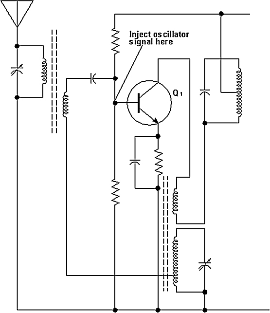
Injection of oscillator signal directly into the circuit
- A quick way to check the oscillator is to position another receiver back to back with one receiver as shown.
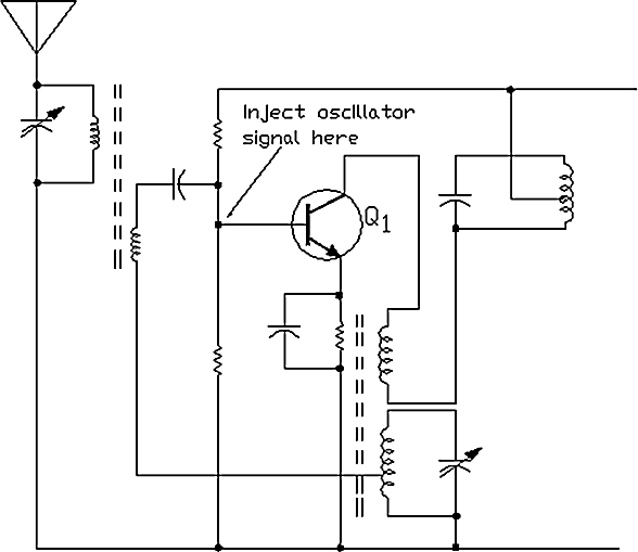
Checking the oscillator
- Consider receiver B as a good receiver. The volume control of receiver A is turned up, and tuned to a strong local station. The volume control of receiver B is turned down all the way and it set to the same station.
- Under this condition the local oscillator of receiver B will inject a radiated signal into receiver A. In most cases, receiver A will begin to play. You may have to move the tuning adjustments of receiver B back and forth to use this trick.
- It is a simple and quick way to determine if the oscillator is working in the receiver being serviced.
- One more example is a two stage audio amplifier which is completely dead. Here an AF (audio frequency) signal must be used. This would be first applied across the loudspeaker and its level adjusted until it is heard as a tone from the indicator, i.e. the loudspeaker. This will prove that the indicator is working fine. Refer to the following figure:
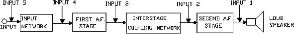
Signal Injection Testing
- Now, the signal is applied at input 2. The signal level must be lower than that applied at the loudspeaker to get the same response. If there is no response, then it means that the second AF stage is defective. Similarly we progress along the chain until we locate the defective stage.
7.5 Signal Tracing
What is Signal Tracing?
- In this technique, a signal is injected at the input and the path of the signal through the system in traced. In signal injection, the signal is injected at each stage ant the output is monitored. However in signal tracing the signal is injected at the input itself.
- This method speeds up the fault finding process. It includes equipment called Fault Traer which has its own indictor. This may be as simple as a headphone. Usually the oscilloscope is an ideal signal tracer. The idea is to trace the signal between the input and the output at various points, by sampling the signal.
- In order to trace the signal a good oscilloscope is used with the help of which you can look at the signal at various points along the signal path. Refer to the following figure:
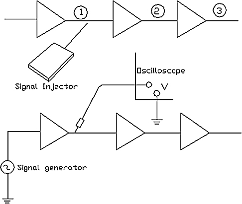
Signal tracing
- If the system is an audio system, then instead of an oscilloscope, a speaker or a headset can be used to trace the signal.
Examples of Signal Tracing
- In signal tracing, the injected signal has to be traced throughout the system. So for this purpose, special signal tracing equipment has been manufactured.
- Let us take an example of a Radio System. The signal tracer actually consists of all of the stages that are available in a radio. Refer to the following figure:
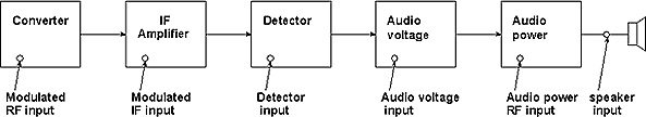
A signal tracer, form of a radio
- So, you probe various parts of the receiver with a switch delivering the signal to the corresponding part of the signal that is in the signal tracer.
- Referring to the above figure, suppose that you are looking at the output of the detector that goes to an audio voltage amplifier. Your signal tracer would be switched to deliver the signal from the output of the detector to the voltage amplifier of the signal tracer. If you get a signal there, you can conclude that everything from the antenna to the detector is working fine.
- However the systems of this type of signal tracing equipment become very sophisticated and expensive. This is true for industrial electronic test stations where the equipment is specially designed and put in rack mounts. In some applications this technique is preferred over signal injection.
- One more example can be of a two stage audio amplifier. It can be tested by first connecting the tracer to the source of the signal, in this case the pickup. This pickup is then connected to the input if the first stage, then to the input of the second stage and then finally to the output of the second stage. The following figure shows this example:
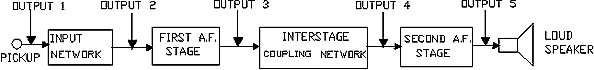
Example of signal tracing in two stage audio amplifier
- An oscilloscope is used to analyze the output, with the help of which we can locate where the fault is.
7.6 Summary
Most of the time, electronic circuits are sensitive to temperature; the reason for this is that the components used in the circuit have some characteristics which are temperature dependant. Hence temperature plays an important role at the time of construction as well as operation of the electronic circuit.
Thermister and sensistor compensation are used against temperature variations. A thermister is a device with a negative temperature coefficient, and a sensistor is a device with a positive temperature coefficient.
The methods of Signal Injection and Signal Tracing are especially useful for troubleshooting systems that have no output. There is a simple device called signal injector which injects a pulse or a wave (square) into the system being tested.
In a signal tracing technique, a signal is injected at the input and the path of the signal through the system in traced. An oscilloscope is used which gives the visual effect of the signal being traced.
There are many phenomena which can cause a considerable amount of error in electronic systems, for example, noise, intermittent, EMI/EMC and so on. This chapter gives a brief idea of all these types of noises and how they are avoided.
The Boltzmann’s constant is also introduced which is used in a mathematical expression to calculate the amount of Noise Power and Noise Voltage.
Learning objectives
- Understand general concept of noise
- Study resistor noise
- Know what is Boltzmann’s constant and noise power and noise voltage equations
- Study various types of noise
- Know the source of noise and troubleshooting
- Study of intermittent and EMI/EMC
8.1 Noise
- In an electronic system, much of the noise is generated by resistors, diodes, transistors and other semiconductor devices. In a communication system (receiver), most of the noise which is created internally is generated in the front end.
- In a television receiver, almost all of the troublesome noise is generated in the television tuner. The noise shows up as snow on the picture and it causes a hissing noise in the speaker. The atmospheric interferences such as lightning create noise that is generated outside the system.
- The amount of snow on television screens, due to internally generated noise is indirectly related to the strength of the incoming signal. A strong signal can override noise voltages. If the signal-to-noise ratio (SNR) is high enough, the noise problem is eliminated.
- In an audio communication system, the noise shows up as a hissing sound in the speaker. In digital systems and microprocessors, the internally generated noise is seen as grass on an oscilloscope display of the signal. Also, it can cause undesired triggering.
Resistor Noise
- In order to understand the concept of resistor noise, let us take an example of a perfect amplifier. A perfect amplifier is the one which increases the amplitude of an input signal, but it does not add any noise to the signal output.
- When there is no input signal and if the wattmeter is connected to the output terminal, then it will show no power output in a perfect (ideal) amplifier. But in a practical amplifier, the wattmeter would show some output power without an input signal. What can be the reason?

A perfect amplifier
- The reason is the noise which is generated within the amplifier. If a resistor is connected across the input of the amplifier, as shown in the following figure, then the output wattmeter shows a measurement, even though the theoretical amplifier still does not produce any noise. This output measurement is known as Noise Power:
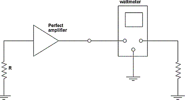
A resistor causes noise in amplifier
- The noise power is generated because the amplifier increases the amplitude of the noise generated by the resistor.
- In the above circuit no current flows through the resistor R. Obviously then the noise is not created by electrons ‘ bumping into atoms and other electrons’ as they move in a current flow. Then, where does the noise come from? The following discussion helps you out! Consider the model of a resistor as shown below:
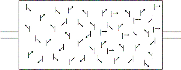
A model of a resistor at room temperature
- Let us not apply any voltage to this resistor by an outside source of power. The atoms in the resistor are in continuous motion called “Brownian Motion “, at room temperature and at all temperatures above absolute zero.
- At room temperature some electrons escape from the atoms for a short period of time. They continuously flow through the material until they are absorbed by another atom that has already lost an electron.
- The current caused by this type of motion of the electrons for a very short duration of time is called intrinsic current.
- The electrons move randomly in the material. But at any specific instance of time there will be more numbers of electrons moving from one direction to another. At that instant of time a voltage drop is created across the resistor.
- When the temperature of the resistor is increased, there will be more numbers of electrons moving in the intrinsic current. A voltage is developed across the resistor, whenever the net amount of intrinsic current flowing in one direction is greater than that flowing in the other direction. The higher the temperature, the higher the amplitude of the voltage. This is because at higher temperatures there is more intrinsic current.
- The voltages created by the random electron flow in the resistor result in fluctuations over a period of time. Hence for the above amplifier, there is a random fluctuation of voltage at the input.
- The random fluctuation is amplified by the (perfect) noiseless amplifier and creates the output noise power. Most amplifiers have resistors at their input terminals and those resistors will produce noise. This noise is very troublesome in some systems. If the noise is greater in amplitude than the incoming signal, then the SNR (signal-to-noise ratio) is very unsatisfactory.
Note
- Any resistor, conductor or semiconductor device connected across an input of a small signal amplifier (that is an amplifier with high voltage gain) will introduce noise into that amplifier. When troubleshooting noise, you should start by going to the source of the signal.
- If an amplifier suddenly begins to produce output noise, the noise is not necessarily caused by a change in the input resistance. However, there is always a possibility the amplifier gain can be reduced. A change in gain can also change the signal-to-noise ratio to a considerable value.
Boltzmann’s constant
- The amount of noise depends upon some very basic theoretical considerations. Boltzmann’s constant can be used to calculate the amount of noise to be expected from a resistor or other semiconductor device.
- Boltzmann’s constant is often denoted by ‘k’ and it is a multiplier for absolute temperature ‘T’. That makes ‘kT’ a unit of energy.
- The amount of noise generated by a resistor increases with temperature. That is because the atoms have more energy at higher temperatures. The energy levels as expressed is kT
- The amount of noise generated in the devices like resistors, diodes, transistors and other semiconductor devices is directly related to the energy of the atoms and electrons. Using Boltzmann’s constant, we can find out the amount of energy and hence the amount of noise that will be created in various components.
- The noise power equation is given as follows:Noise Power = kTB watt
Where:k is Boltzmann’s constant
T is absolute temperature in degrees Kelvin, and
B is the bandwidth in Hz - The equation of noise voltage generated in a resistor is
Where:k is Boltzmann’s constant
T is absolute temperature in degrees Kelvin
B is the bandwidth in Hz, and
R is resistance of the resistor - Many names are given to the noise generated by a resistor at room temperature: Johnson’s noise, thermal noise, thermal agitation noise, or white noise. White noise gets its name because it supposedly contains all audio and RF frequencies, as in the case of white light which has all visible frequencies. Pink noise has more numbers of lower frequencies than higher frequencies. A semiconductor diode is also a good source of white noise. Both the equations given above show the effect of temperature on the noise created in a system.

Distribution and Types of Noise
- The equations for noise power and noise voltage show that the amount of noise is directly proportional to the bandwidth of the amplifier. Hence, the amount of noise can be increased by increasing the bandwidth of the amplifier. Also, increasing the resistor will also increase the amount of noise injected:
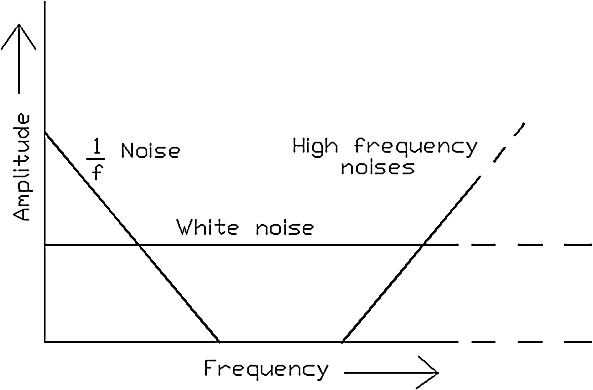
Types and distribution of noise
- The above figure shows the types of noise and their distribution in a typical electronic amplifier. White Noise has constant amplitude throughout the bandwidth.
- 1 / f Noise: When current flows through the resistor, very small instant-to-instant changes in current cause a varying type of noise. This is a source of 1 / f Noise.
- Similarly, in a vacuum tube, when the cathode is heated, electrons are emitted from its surface. At any instant of time the number of electrons leaving the cathode will be different from that at any other instant. That produces a special kind of noise known as Flicker Noise or 1 / f Noise.
- Flicker noise is primarily a problem at the low frequency end of the spectrum. It is present in all amplifying devices. It decreases in amplitude when the frequency is decreased.
- There is one more noise called Partition Noise in amplifying devices. Considering a bipolar transistor, we can say that some amount of the electrons which are leaving the emitter area goes to the base and the rest goes to the collector. Refer to the following figure:
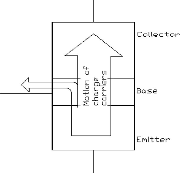
Partition Noise in bipolar transistor
- From instant to instant the number that goes to the base as opposed to the number that go to the collector changes in a random way. It means that the base current changes from moment to moment by a very small amount.
- This variation becomes the source for transistor noise. The small base current changes are amplified due to transistor beta. So there exists a considerable amount of amplified output noise in the total amount of amplifier noise.
- In vacuum tubes there is also a problem of partition noise:
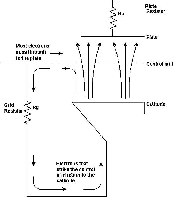
Partition Noise in vacuum tubes
- The above figure shows a triode vacuum tube internally. You can see the electrons sticking to the control grid and returning to the cathode through the grid resistor. The number of electrons that actually flow through the grid circuit is subtracted from the output plate current. So there is a moment-to-moment change in current through to the plate resistor.
- These variations in the partition current flowing through R cause a noise voltage to appear across that resistor. The noise voltage is amplified by the tube
- There is no partition noise in JFET and MOSFET. The reason being that there in no motion of electrons in the gate region in these devices. This is the reason why FET transistors are used extensively in modern communications and other high frequency electronic systems.
External Noise
- External noises, as the name suggests, they occur external to the system. Usually it is some form of external noise. Examples include static created by lightning and noise generated by machinery.
- Impulse nose, as with any other pulse, contains a very large number of harmonic frequencies. It is great disturbance in electronic systems.
- Not much can be done about impulse noise for a given system. Some intelligent use of antenna theory may help. You can incorporate coaxial cable to prevent the impulse from being picked up by the transmission line. The shield prevents the line from being picked up by the antenna.
- Impulse noise is usually horizontally polarized, so long horizontal runs should not be used in a receiver antenna system.
Finding a Noise Source and Troubleshooting
- Consider a system is working fine at one time and suddenly it requires servicing because of internal noise. This may be due to a transistor that has had a beta change that reduces the signal to noise ratio. It could also be due to a bad component such as when a resistor becomes too hot.
- Now, how to find the source of the noise? Assume that all the preliminary tests have already being done and power supply voltages measured. A low power supply voltage can cause a reduced amplifier gain and a reduced signal-to-noise ratio.
- Troubleshooting can be started with defeating all the closed loop circuits in the system. If the system has an automatic gain control and automatic frequency control, it is important to defeat that circuit.
- The automatic gain and frequency control carry noise signals in a feedback loop because of the wide bandwidth of the noise. So, it becomes necessary to defeat the automatic frequency control as well as automatic gain control.
- The best way to do that is to replace the DC voltage in the feedback systems with a DC supply voltage preferably from a battery pack that will not add hum or noise.
- The negative feedback is used in many applications such as industrial speed controls, hearing aids, public address systems and so on. Mainly the negative feedback is used in receivers. In all these systems, when you are looking for the source of noise, the feedback circuit must be located and defeated.
- After you defeat all of the closed loop systems, begin to look for the noise source by starting at the input of the system. This is done because the noise is created at the input end of the system. Do not start in the middle of the system for this type of troubleshooting.
- For example, in a communication system, start at the antenna terminals, in an industrial system, start at the transducers, in an audio start at the microphone.
- Moving away from the input, disable the circuit one at a time. If the noise stops, then the noise source is in front of the circuit you just disabled. Disabling the circuit usually means to ground the signal input or, in case of bipolar transistors, short the emitter to base.
- As you move through the system, listen to the output noise. This is best done by turning the system gain to the maximum value, and at the same time defeating the input signal from the transducers, antennas, or other signal source. When you move past the offending circuit, the amount of noise in the output should be much lower.
- There is one more method of finding the noise. It includes signal injection and signal tracing. The method is to think of the undesired noise as being an injected signal. Use the signal tracing method to find the source. You can start in the middle of the system and work towards input. While going towards the front end, you can pass through the source of the noise. This helps you discover where the source of noise is located.
Minimizing the Noise
- Grounding is one of the primary ways to minimize unwanted noise and undesired signals. A good ground system must be designed for this purpose. The advantage of a good grounding system is that it minimizes the noise voltage generated by currents from two or more circuits, which are flowing through a common conductor.
- At low frequencies typically below 1MHz, a single point ground system should be used. Refer to the following figure:
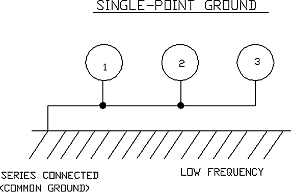
Common ground system
- At high frequency, typically above 1MHZ, a multipoint ground system should be used as shown in the following figure:
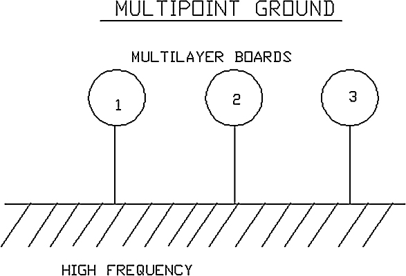
Multipoint ground system
- Care should be taken while grounding that ground loops and differences in ground potential are avoided. For good grounding system, keep the signal traces short and direct to avoid their acting as receiving antennas.
8.2 Intermittent
- You have to equally worry about the intermittent as you are worrying for the noise. It can be a very frustrating problem in electronics. Now what is the form of this intermittent? Intermittent faults don’t remain long enough to trace and isolate and they reappear suddenly.
- A switch that turns a signal on and off in a system suddenly, then that switch is said to create intermittent in the system. So, the switch has to be located in order to overcome the intermittent.
- The variety of sources of intermittent is endless. But some of the intermittent problems include a break in the printed circuit board, a cold solder joint, and a defective tube, transistor of FET, a broken wire or an intermittently shorted component.
- Intermittent faults can be caused by poor connector contact, broken wires; loose bits of metals on the PCB shorting the track, bad solder joint, loose ground connection, defective insulation between conductors and so on.
- Power supply can also be a source of intermittent. When you have a suspicion about intermittent, it is a good idea to disconnect the power supply and substitute the battery pack. Check and compare the output on oscilloscope.
- Like noise source, intermittent are also difficult to locate if you do not defeat the closed loop feedback circuit within the circuit. This is the first thing to do after performing the preliminary checks and measuring the supply voltage.
- For troubleshooting of intermittent, start at the input end, and look and listen for the intermittent as you move through the system. While doing this, it is a good idea to slightly flex printed circuit boards and move components with an insulated stick to try to stimulate the intermittent.
- By analyzing the symptom and with a block diagram concept of the equipment, the approximate area where the failure may have occurred can be determined. Make a note of when the fault occurs to identify the probable cause.
- Many a times, intermittent are temperature dependants. So it is advisory to use a heat source such as a hand held hair dryer, to heat different sections of a circuit as a method of inducing or stimulating the intermittent action.
- The question is why they are stimulated? Some intermittent only occur at high temperatures. For example, when the system is in its cabinet, it will display intermittent behavior, but when it is out on the workbench, the cooler ambient temperature prevents the intermittent from occurring.
- Super coolant sprays or components can be used to stop noise or intermittent interference. A Freon spray can be a good choice. It stops the intermittent of the type that occurs at high temperatures.
Caution
When you are using super coolant, you have to be careful, because it can produce instant frostbite! Furthermore, if inhaled into lungs strongly, they can cause permanent lung damage.
8.3 Sources of Interference
- There are two types of interferences: continuous and intermittent. The most common continuous noise source is hum, caused by a supply power.
- Radio frequency noise can be caused by local radio, television stations, and radar and ham radio stations.
- Wideband noise is caused by a high power electric motor. They radiate noise into almost any equipment that is in close proximity to the motor. The SMPS in DC motors can cause high frequency noise through common power ground. When the motor ramps up and down, the noise can vary in frequency and power.
- SMPS (Switch Mode Power Supplies) can cause high frequency noise through common power ground. They create large amounts of harmonic frequencies. The power supplies develop low voltages from mains power by switching the high voltage on and off very quickly, this creates lots of noise. The wires that connect the power supply to the device then transmit this noise.
- Ignition circuits in motorcycles, cars and other gasoline powered motors put out wideband noise created by tens of thousands of Volts. Microwave ovens radiate wideband noise by leakage through edges of the door or from the power supply wires. The oven can transmit hundreds of watts over short distances.
- Static devices, arc welding, lightning, switch relay equipment, etc are the causes of intermittent noise.
8.4 Static Discharge
Many a time the unprotected environments fall pray to static voltages. These static voltages ranging from 1kV to 30 kV can be present in such environments. Static discharges can damage some electronic components. Care should be taken in order to avoid the effects due to static discharges.
- If any package contains some static sensitive devices, then the package should be labeled clearly.
- Minimize handling of static sensitive devices.
- The component leads of such devices should be kept shorted together, wherever possible.
- Never touch the component leads. The component can be picked up by its body instead of lead.
- Transport and storage of such components should be done in their original packing or on metallic rails.
- The things which generate or hold static discharge should not be brought near to the workstation.
- Static voltage discharge from the human body can be reduced by wearing a grounded antistatic wrist wrap while handling these components.
- Servicing of static sensitive components should be done in a static free work station by a qualified person.
- A soldering iron which is connected to ground should be used. For de-soldering, an antistatic de-soldering pump is used.
8.5 EMI / EMC and its sources
- Electromagnetic interference (EMI) and electromagnetic compatibility (EMC) problems should be prevented to ensure a good performance of the system. The equipment which are highly sensitive become affected due to electromagnetic radiation or interference. The source of electromagnetic radiation can be nearby electrical or electronic equipment, conductors, transmitters etc.
- It is also referred as RFI, radio frequency interference, and it is harmful because it acts on sensitive electronic circuits in a way that is similar to direct sunlight acting on photographic film.
- Many a time the frequency of the electronic signals is above 100 kHz, because of which the electronic signal just seem to leap out of the ordinary wires that were supposed to contain them. These ordinary wires become radiating antennas.
- Active and passive components can both be the source of EMI, depending upon the signal frequencies and characteristics of the component. At high frequencies the active components may become a direct radiator or receptor of EMI. The component’s power and ground connection can provide a path for emission.
- An inductor can become predominantly capacitive because of the coupling between the windings which can be a high frequency parasitic coupling. Also a capacitor can develop parasitic series inductance due to its internal inductance and external lead inductance at high fundamental harmonic frequencies.
- Electromagnetic compatibility (EMC) means that the device is compatible with its electromagnetic environment and it does not emit any electromagnetic energy which can cause electromagnetic interference in neighboring devices.
- In digital circuits, the source of emission can be fast clock, switching gates and periodic waveform. The cross-talk depends directly on the clock rate. If the clock rate is doubled, the cross-talk is increased by a factor of two.
- To get rid of EMI, designers usually enclose the most sensitive parts of a circuit in a metal box.
Types of EMI
There are four basic types of EMI as follows:
- System Radiated EMI
- External Radiated EMI
- Internal Radiated EMI
- Conducted EMI
System Radiated EMI
The following figure shows electromagnetic interference. Here the system itself is the source of EMI:

System radiated EMI
External Radiated EMI
The source of the interference is outside the system. Refer to the following figure:
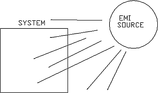
External radiated EMI
Internal Radiated EMI
The source of the interference is inside the system. Refer to the following figure:
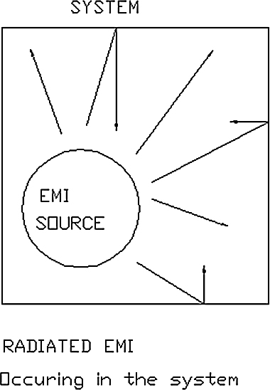
Internal radiated EMI
Conducted EMI
Here the electromagnetic energy can escape from the source conducting along wire and cable leaving equipment. The following figure shows conducted EMI:

Conducted EMI
Shielding, Filtering, Bypassing
- Shielding is a process aimed at confining radiated energy to the bounds of a specific region or to prevent radiated energy from entering a specific region. It has been found that the shielding of source is required more as compared to the shielding of receptor, because source is the one which is allowed to radiate (for example, Broadcasting stations).
- Shielding is accomplished by two mechanisms: absorption loss and reflection loss. At low frequencies, shielding is accomplished primarily by absorption loss and at high frequencies it is accomplished by reflection loss. However, the total shielding function is a composite of both reflection loss and absorption loss.
- The thickness of the shield can be calculated by simplifying these two phenomena. There is a unit of measurement for shielding called ‘one skin depth’. This is the thickness of the piece of metal which is bombarded with EMI.
- A total closed shield isolated from outer world is never possible. The source has to have connections from the outside systems which are power system and load terminals. The shielding can be in a form of partition boxes or cable and connector.
- A shield reduces EMI field strength. Shielding is measured and specified in terms of reduction in field strength caused by the shield. A material which is used for sealing seams and joints on shield to prevent EMI energy from passing through it is known as EMI gasket.
For example, the following figure depicts a PC board without filtering or shielding:
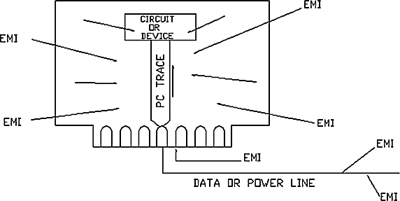
PC board without filtering or shielding
- The electromagnetic energy enters the device along cables and traces by radiation through the air. When filter capacitors are installed, conducted interference is reduced. These filters conduct the desired current but reject the undesirable currents. However, energy can still enter the source by direct radiation.
- A shield prevents the radiated EM energy from interfering with the equipment. Thus both filtering and shielding both are necessary to prevent possible EMI problems. With the same purpose as with shielding, filtering is used to solve EMI problems when the circuit is the source of noise. The following figure shows the effect of shielding and filtering:

Effect of filtering and shielding
- The discrete capacitors and bypass capacitors should be placed as close to the voltage source as possible and adjacent to the active devices if present. In digital circuits, capacitors filtering low frequency supply voltage noise are generally placed adjacent to the voltage input pins. The value of such capacitors can be 10µF or above.
- Capacitors filtering high frequency noise should be placed at the IC being filtered. These capacitors are low value capacitors of the range 1µF and below. The ideal position of the capacitor and the IC would be across the supply voltage and ground pins.
- EMI filters can be used as a shunt element to divert electrical currents from a trace or conductor; as a series element to block a trace or conductor current; or they may be used as a combination of these functions. Selection of the filter elements should always be based on the desired frequency range and component characteristics.
- To filter a signal and to isolate the power source using decoupling, a capacitor is the best signal filter within its high frequency performance characteristics. The bypass capacitor greatly reduces the power and ground circuit noise, if they are located properly in design layout.
- EMI problems at high frequencies can be reduced by using a low pass filter. It incorporates a capacitive shunt and series resistance or inductance. However, at high frequency, the capacitor can become inductive and the inductor can become capacitive causing the filter to act more like a band-stop filter.
- The basic criteria to design a filter should be based on the overall impedance at the circuit’s point of application for proper match. For most EMI applications, a T-filter design is effective and is ideal for analog and digital I/O ports.
Precautions
- Cross-talk and EMI radiation can be reduced by minimizing the PC board trace height above the ground plane. Parallel traces are adopted to reduce cross-talk. The two parallel traces should be separated by at least two trace widths for cross-talk reduction.
- Multilayer printed circuit boards are used instead of single layer whenever possible. A ground plane should be used for a single layer PC board to reduce radiation.
- Power and return planes should be located on opposite sides of a multi-layer PCB. The power planes being low in inductance, any transients that may develop on the power planes will be at lower levels, resulting in lower common mode EMI.
- Locate analog and digital circuits on different layers, because both the circuits can interact if placed close to each other. If it is unavoidable, digital and analog areas should be properly isolated. The clock and oscillator components should be properly shielded with foil or small metallic enclosures.
- While designing a capacitive filter, capacitor lead and trace lengths must be short at the high frequencies in order to prevent the addition of inductive reactance. Use ceramic capacitors at high frequencies in GHz range.
8.6 Cross-Talk
Introduction
- In simple words, crosstalk is defined as a disturbance, caused by electromagnetic interference, along a circuit or a cable pair. It causes reduction of signal strength during transmission. It is also known as interference in a communications channel caused by activity in other communications channels.
- Another term which is known as “Alien” crosstalk is defined as the interference that comes from a wire in an adjacent cable, for example, when two or more twisted wire pair cables are bundled together.
- In electronics, crosstalk (XT) means undesired capacitive, inductive or conductive coupling from one circuit, part of a circuit or channel, to another. It also means any phenomenon by which a signal transmitted on one circuit or channel of a transmission system creates an undesired effect in another circuit or channel.
- In telecommunication or telephony, crosstalk is often distinguishable as a piece of speech or signaling tones leaking from other people’s connections. A telecommunication signal disrupts a signal in an adjacent circuit and can cause the signals to become confused and cross over each other.
- In integrated circuits, crosstalk normally refers to a signal affecting another nearby signal. As compared to analog, the digital signals are less susceptible to crosstalk.
- Crosstalk causes attenuation in signals. Attenuation is the opposite of amplification, and it occurs whenever a signal is transmitted from one point to another. But, if the signal is attenuated too much, it becomes weak and unintelligible. To reduce this effect, repeaters are employed at regular intervals in most networks.
- Attenuation is measured in decibels (db). Attenuation to crosstalk ratio (ACR) is a factor which determines how far a signal can be transmitted in any given medium. It is the ratio of the attenuated signal to near-end cross talk (NEXT). NEXT is one of the types of crosstalk which is discussed below.
- ACR is the difference between attenuation and crosstalk at a given frequency along a cable. It assures that a signal transmitted along a cable is stronger at the receiving end than any interference signals imposed on the cable by crosstalk from adjacent cable.
Types of Crosstalk
There are three major types of crosstalk:
- Near-end crosstalk (NEXT)
- Far-end crosstalk (FEXT)
- Power sum near-end crosstalk (PSNEXT)
Near-end crosstalk (NEXT)
As the name suggests, Near-end crosstalk occurs near the transmitting device. A signal is applied to one pair of wire and cable and the amplitude of the induced signal along the other wires is measured. It is more troublesome than far-end crosstalk.
Far-end crosstalk (FEXT)
Far-end crosstalk occurs towards the end of the cable run. Here the distance matters and the signals that are transmitted get weaker with distance. The effects of FEXT are less severe than NEXT.
Power sum near-end crosstalk (PSNEXT)
It comes into picture when more than two pairs of wires are transmitting data. PSNEXT measures the cumulative effects of NEXT from all of the other wire and cable pairs.
Some other types are also discussed below:
In direct crosstalk, the disturbing channel couples to the disturbed channel, and in indirect crosstalk, the coupling path between the disturbing and disturbed channels requires the third or tertiary channel. Interaction crosstalk (IXT) is a term used to describe indirect crosstalk that couples from the disturbing channel to the tertiary channel at one place prorogates along the tertiary channel, and subsequently couples into the disturbed channel at another place. Transverse crosstalk (TXT) is a term that includes all direct and indirect crosstalk that is not interaction crosstalk.
Remedies to reduce crosstalk
- When a signal is traveling along wire and cable, then the voltage level changes and this change in voltage level is represented binary 1s and 0s that will be understood by the receiving host. But changes in voltage levels produce electromagnetic energy, which can be absorbed by nearby wire and cable.
- The net effect of this can be interference on the wire and cable that results in an unstable network. In order to reduce the effect of this interference, the first job is to find out what is the source of interference and then take corrective actions to reduce their effects.
- To reduce crosstalk, the techniques for decreasing coupling among the communications channels are adopted. In multi-pair cables, twisted pairs are used. Shielding of coaxial conductors, use of optical fibers in place of pairs are some techniques for reducing electromagnetic coupling where space division alone is not adequate.
- The systems which are based on frequency division method, improved control of signal levels and improved linearity in amplifiers, are effective. The amount of crosstalk can be reduced by proper selection of modulation techniques. One should be able to decide which modulation technique, Amplitude, Frequency, or Phase modulation to be used, which depends upon the system.
- In a multi-channel digital system, especially those which transport digital versions of analog signals, the crosstalk is reduced by employing a separate coder-decoder for each analog channel. Usually, a common, time-shared coder-decoder is used for all channels to reduce extra circuitry.
An Example of Crosstalk
Let us see an example of crosstalk between oscilloscope channels. If there is a crosstalk between channels of an oscilloscope, it may result in a measurement error. The following figure shows inter-channel crosstalk in oscilloscope:
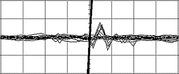
Inter-channel crosstalk in oscilloscope
- In an oscilloscope, inter-channel crosstalk is said to occur whenever a large signal such as a logic signal is displayed on a scope, at the same time a small signal is also displayed on another channel.
- The above figure shows two traces, one a large signal and the other a much smaller signal displayed with persistence to show several traces. Because of inter-channel crosstalk, an error signal is generated on the sensitive trace. In this case, the crosstalk is only on adjacent channels i.e. channel 1 and channel 2, not on channel 1 and 3 and only when a large signal is driven off screen. The large signal is 300mV peak-to-peak.
- If the scope is driven with multiple signals, each signal should be kept within the range of the screen, even if not currently being displayed.
8.7 Summary
In an electronic system, much of the noise is generated by resistors, diodes, transistors and other semiconductor devices.
SNR (signal-to-noise ratio) is an important term to know the amount of noise. If the (SNR) is high enough, the noise problem is eliminated.
Boltzmann’s constant is used to calculate the amount of noise to be expected from a resistor or other semiconductor device. Using Boltzmann’s constant, noise power and noise voltage can also be calculated.
White noise, Flicker noise, partition noise are the types of noise.
The chapter gives an overview of the soldering techniques for repair and replacement of components. It explains the process of soldering, soldering tools and so forth. Also it flashes common faults in professional soldering, and how to recognize a good and bad solder connection. De-soldering technique is also explained.
Learning objectives
- Study the basic process of soldering
- Study of soldering tools, cleaning tools, solder and flux
- Know how to form a component
- Understand temperature aspects in soldering
- Differentiate between good and bad solder joints
- Study the process of de-soldering
- Know some practical tips in soldering and de-soldering
9.1 What is soldering?
- In the production of electrical and electronic equipment, the joining of metal surfaces by soft soldering to produce a good mechanical bond of low electrical resistance is an essential feature.
- Soldering is an art, it is a technique. For locating a problem in the functioning of a circuit, sometimes it is necessary to remove or add a component from the printed circuit board and carry out the requisite tests on it.
- Soldering involves removal and replacement of the electronic components from the printed circuit boards. If a component is soldered, it means that there is a continuity of metal. Soldering is an alloying process between two metals.
- It is a popular method of connecting circuits. When it is done properly, soldering is a highly reliable and low cost process. Most of the solders used today are 60/40 type, i.e. 60 percent tin and 40 percent lead. A better is 63/37 variety which has 63 percent tin and 37 percent lead. This alloy is available in wire form and in several gauges.
- Most combinations of tin and lead become plastic before they actually melt. So they have three states: solid, plastic (mushy) and liquid. 60/40 is the plastic state, but there is a very small difference between the liquid and solid state.
- The 63/37 solder is eutectic at a temperature of 370 O. This means that it goes directly from the solid to the liquid state without having a plastic intermediate step. This is one of the reasons that 63/37 are often used for replacing parts on newer systems where components are very small and sensitive to heat.
- The following figure shows the difference between 60/40 and 63/37 when heated:

Solder and their melting temperatures
- Plastic solders are also available. Instead of soldering with a combination of lead and tin, plastic solders can be used which are soft in state and are hardened by heat or by adding a chemical called a catalyst or hardener. In either case, the plastic solder is applied first and then hardened.
- The plastic solders which use catalyst for hardening are useful in surface mount configurations, where heat must be used sparingly to protect the component. Plastic solders form a solid, strong bond and they are easy to apply.
- There is one more type of solder called silver solder which employs indium. Another type of solder combines indium, tin, lead, cadmium and gallium. These solders melt at very low temperatures, but they do not flow easily like the more conventional solders. Some solders melt at such low temperatures that they can be melted with the flame from a match.
- In its molten state, solder dissolves some of the metal with which it comes into contact. The metals to be soldered are more often than not covered with a thin film of oxide that the solder can not dissolve. A flux is used to remove this oxide film from the area to be soldered.
Caution
Cadmium is a highly poisonous material. Never inhale any smoke from soldering. In fact, a small fan should be part of your bench equipment, to push the smoke away from you while you are soldering.
9.2 Process of Soldering
The process of repair of any electronic circuit involves following these major steps:
- Dis-assembly of particular component
- Testing of the component
- Replacement of the component found defective and
- Testing the circuit for performance check
A good soldering practice is required for the removal and replacement of electronic components. The soldering process involves:
- Melting of the flux which, in turn, removes the oxide film on the metal to be soldered
- Melting of the solder which makes the lighter flux and brings the impurities suspended in it to the surface
- The solder partially dissolving some of the metal in the connection and
- Cooling and fusing with the metal
The soldering process needs an understanding of:
- Soldering tools
- Soldering material
- Soldering procedure
- Replacing components
- Special consideration when using MOS and micro-electronic circuits
- Good and bad soldering joints and
- De-soldering techniques
The process of soldering requires the following steps:
- The soldering iron must be placed at an angle of 45O to the soldering area
- The solder is placed near the iron and it is flowed. It is passed around the joint until you come back near the iron
- Now let the solder flow into the area from where the iron has been removed
- All the elements of the joint must be covered with the solder. The joint formed by the solder must be firm
- The solder is taken away when it is ensured that the solder has flowed into the leads and tracks. First the solder is removed and then the iron is taken away. If the iron is removed first, it will result in a dry joint, due to the solder taking heat from the joint prematurely
9.3 Soldering Tools
Many tools are available to facilitate soldering work. The most essential tools used in soldering practice are discussed below:
- Soldering Gun
- Strippers
- Heat Sinks
- Cleaning tools
Soldering Iron
- It is the most important tool used in the process of soldering. The main function of a soldering iron is to supply sufficient heat to melt solder by heat transfer when the iron tip is applied to a connection to be soldered.
- Soldering irons come in two categories: Solder Pencils and Solder Guns. The type of the soldering iron should be selected on the basis of its tip size, shape, operating voltage and wattage. The temperature of the soldering iron should be selected and controlled according to the work requirement.
- Let us see both the types one by one.
Solder Pencils
- Soldering pencils are one of the very light weight soldering tools. They are suitable for almost all types of heat generation requirements. The soldering pencils can generate as little as 12 watts or as much as 50 watts of heat. The following figure shows a soldering pencil:

A Soldering pencil
- A pencil type of soldering iron takes a few minutes to attain working temperature. A typical soldering pencil has a handle, a heater recess, a heater, a tip and a tip retainer.
- The heater recess gives a strong base to the heater for heating. Modular soldering irons use inter-changeable heating elements and tips which fix to the main body. Such elements screw into a threaded receptacle at the end of the pencil.
- The soldering task can be a very fine one, so that almost a needle type of tip is required on the printed circuit board for IC component foil pads which are closely placed. Some shapes and sizes of the tips are shown:
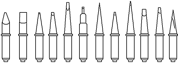
Pencil Tips
- The connectors which are widely spaced, require a greater amount of heat, so larger, chisel and pyramid type tips are used. Bent chisel tips can get into difficult-to-reach areas.
- It is better to keep the pencil continuously powered even for interrupted type of soldering works. This requires keeping the iron in a safe place at the working temperature. You can keep it in special soldering iron holder which may be a coiled steel form into which a hot soldering iron can be inserted.
Solder Guns
- The solder gun is a type of soldering iron which generates more heat and it comparatively heavier than the pencil type of soldering iron. The following figure gives a picture of solder gun:

Soldering Gun
- They are called pistols because they resemble pistols. The gun’s trigger is actually a switch that controls the application of AC power to the heating element. Soldering of heavy duty connectors and conductors require the use of guns because it can generate enough heat to quickly bring the heavy metal up to the proper soldering temperature.
- The gun triggers the working temperature instantaneously. Some guns have a multi position trigger switch which can be used to select different heat level.
Strippers
- Strippers are used to remove insulation from the wires. The most employed strippers are those of a cutting type as shown in the figure below:

Wire Stripper
- These strippers are so designed that they can accommodate various sizes of wires normally used in electronic equipments. In order to prevent damage to the wire by nicking, it should be ensured that the specific wire size hole is selected in the cutting stripper.
- In the thermal strippers, the wire to be stripped is placed between two electrodes. The electrodes get heated when electric current passes through them. The resulting heat melts the insulation.
- When using thermal strippers, toxic fumes emanating from compounds such as polyvinyl chloride or polytetra-flouro-ethylene must be properly exhausted by using some type of fan ventilation system.
Heat Sinks
- There are some components such as semiconductor devices, meter movements and some insulating materials which are highly sensitive to heat. They must be protected from damage due to heat while soldering:

Use of pliers as heat sink in soldering
- Devices such as alligator clips, nose pliers, as shown in the figure, commercial clip on heat sinks, felt-tip tweezes, anti-wicking tweezers and other similar devices are usually placed or clamped at the site of soldering. They prevent the heat from reaching the components.
Cleaning Tools
- Alcohol dispenser, camel hair brush, small wire brush, synthetic bristle brush, cleaning tissue, pencil eraser, typewriter erasers, braided shielding tools, sponge with holder, tweezers etc. are the most commonly used devices for cleaning purposes in the soldering process.
- Before the soldering process is actually performed, the surface on the printed circuit board or the component leads must be properly cleaned:
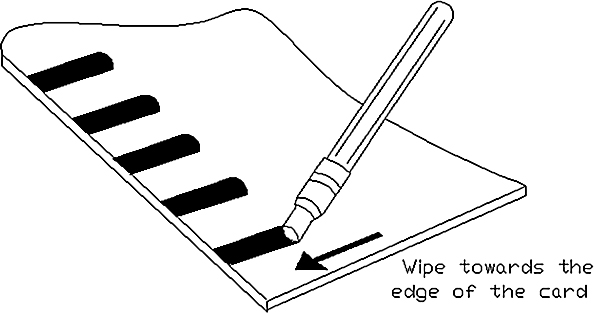
Pencil eraser
9.4 Solder and Flux
Solder
- The material which is used for the purpose of joining together two or more metals is called a solder or soldering material. As said earlier it is an alloy of lead and tin. Sometimes it can contain varying quantities of antimony, bismuth, silver or cadmium which are added to vary the physical properties of alloy. Some popular solders, their melting temperature and states were explained earlier with a diagram.
- The solder alloy is available in a wire form with various gauges. When the alloy consists of 60 percent tin and 40 percent lead, then it is drawn into a hollow wire whose centre is filled with an organic paste like a material called rosin. The resulting product is called 60/40 rosin core solder.
- The solder of 63/37 is abbreviated as SN63. With this solder, the stress resistance of the solder joint is in the maximum, i.e., at the lowest melting point the alloy has the highest pull strength.
- Thinner gauges are preferred over thicker ones. Fine solder is easy to position on the joint and requires less heat for the formation of a joint. The solder alloy wires are commercially available in different diameters ranging from 0.25mm to 1.25 mm. The volume of the flux in the wire is about 25 percent corresponding to a mass of about 3 percent.
- The solder should have a good quality of alloy composition and flux. The lead present in the solder does not cause any health hazard. However, when handling lead dust, a mask must be used. Smoking during soldering may cause lead smoke to be inhaled and this should be avoided.
Flux
- One more substance known as ‘flux’ is used to aid the soldering process. It is required to scrub away the microscopic film of oxides on the surfaces of metals to be soldered. Flux is applied before or during soldering. It forms a protective film that prevents re-oxidation while the connection is heated to the point at which the solder melts.
- It is useful in case of a stubborn joint that would not accept solder. Many metals form compounds with atmospheric oxygen which leaves a coating of oxide even at room temperature. The oxides are removed by fluxes which remain liquid at soldering temperature. They react chemically with the oxides and disperse the reaction products.
- The solder used in most electronic work contains the flux as a central core which has a lower melting point than the solder itself. When molten flux clears the metal, it allows the solder to wet the metal, and, it holds the oxides suspended in solution. The molten solder can then make contact with the cleaned metal and the solvent action on the metal can take place.
- The most convenient solder is the type mentioned above that has the proper flux, usually resin, in the center or core of the solder. With that type the flux is applied every time you solder. The flux is needed for cleaning the surfaces in order to make a better solder connection.
9.5 Component Forming
- Component forming is one of the major procedures in the process of soldering. Component forming secures the lead of the component to the circuit. The component must be properly formed and fit into the circuit in which they are to be installed.
- The leads of the component must be bent with care to ensure proper fixing. A lead should not be bent too close to the component encapsulation. If so, there can be excessive stress at the lead entrance which causes cracks in the encapsulation. Environmental moisture can enter through the cracks and because of that there can be a gradual degradation of the component.
- Following are the guidelines which will be helpful for proper component forming:
- The minimum distance to be maintained between the component body and the bend should be not less than 3-5 mm:
Figure 9.8
Component forming (a), (b) - The radius of the bend should be equal to twice the thickness of the lead wire. The component is inserted in the printed circuit board with the component placed in the centre between its soldering connections:
Figure 9.9
Component forming (c) - The leads are bent by pressing the towards the printed circuit board. Any bending tool can be used. Usually the protruding lead is bent at 45 ό after insertion into the PC board:
Figure 9.10
Component forming (d) - The part of the lead which is exceeding the perimeter of the pad is cut finely, then the lead is pressed firmly. It gives you the final shape of the component leads as the component is fixed on the PC board:
Figure 9.11
Component forming (e) - It gives you the final shape of the component leads as the component is fixed on the board. Care should be taken while bending the lead, that it should not be moved back and forth quickly, because it causes the lead to break or crack.
- The minimum distance to be maintained between the component body and the bend should be not less than 3-5 mm:
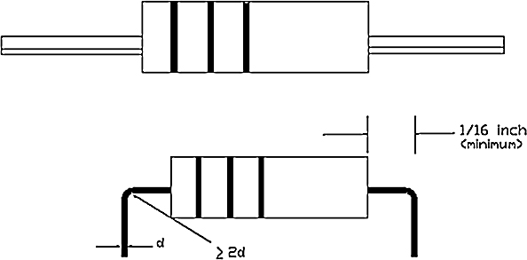
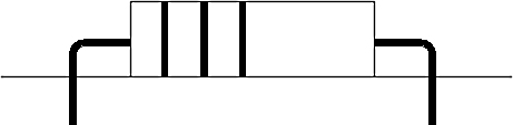
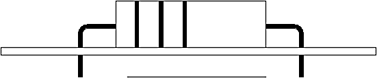

9.6 Temperature Range in soldering
- Temperature is a critical parameter which should be monitored in the process of soldering. Components like semiconductors get damaged because of excessive heating, which subsequently results in premature failure of the circuit.
- Before the process of soldering actually starts, it is advisable to ensure that the temperature of all the parts should be raised to roughly the same level. Heating one part and not heating another will produce an unsatisfactory solder joint.
- Following is the ideal graph of Temperature V’s Time:
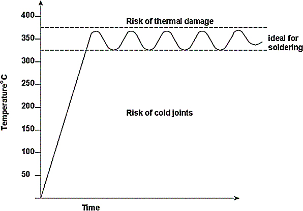
Temperature Range
- The graph shows you the ideal range of temperature for soldering. The temperature of the soldering iron tip is about 330 ό C – 350 ό C. The melting point of the solder is in the range of 188 ό C.
- Above this temperature range, there is a risk of thermal damage, whereas below this range cold junctions can develop. The heating period is also an important factor. Heating for an excessive time period damages the component as well as the copper foil of the component.
- The components which are sensitive to heat should not be heated more than a few seconds. The heating period depends upon the temperature of the soldering iron and the size of the joint.
- Thermal protection devices such as heat sinks and thermal shunts, and coolers can be used while soldering.
9.7 Component Replacement
- It is a very common practice to replace a component from the printed circuit board. However, unnecessary component substitution is to be avoided. When the component is being removed, the solder has to be removed, which should be done with a suction device or wooden toothpick. Sharp metal objects should never be used.
- Before removing the component, information such as polarity, placement angle, positioning, insulating requirement, etc. should be noted to avoid any confusion. Refer to the manual to know the replacement procedure of the instrument. Do not forget to label the components to be removed, so that the removed components will not get mixed with the new ones.
- Before starting the actual removal of the component, switch off the power and remove any assemblies, plugs and wires. If the power is on, it may produce voltage or current surges which can damage the component and other sensitive components.
- Heat the solder fillet, on the solder side of the PC board. The component is removed carefully with a de-soldering tool. For multi-lead components, the vacuum de-soldering tool must be used to remove all the solder from component leads before the component can be removed from the board. This process needs extra care because multi-lead components have more probability to damage the PC board.
- Sometimes the components are inserted using a machine, the removal of which from the circuit board becomes difficult. So, first straighten the leads of the component on the back side of the circuit board using a small screw driver or pliers while heating the soldered connections.
- After removal of the component from the PC board, the area on the printed circuit board must be cleaned up with cotton tipped applicator in a solvent. The plated-through holes must be cleaned for easy insertion of the new component.
- The replacement component should be cleaned; the insulation must be removed in case of wire lead. The leads of the replacement component should be bent in such a way to match the mounting hole spacing.
- Now refer to the record for the previous component for polarity, etc. and insert the component leads into the mounting holes and position the component according to the previous component positioning.
- Using a soldering iron or gun and solder, start soldering. Heat the parts to be soldered, not the solder. The solder starts flowing, when the component leads, wires are hot. Apply the soldering iron to the joint and feed the solder into it.
- Remove the soldering iron and allow the solder to cool and solidify. To avoid a cold solder joint, keep the board undisturbed for a while and allow it to air dry completely.
- In order to test the repaired solder for continuity, you can use a multimeter. The ohmmeter will measure the resistance between the solder and the component lead. If the ohmmeter shows a reading, it means that the joint is defective.
9.8 Inspecting Soldering Joint
In the process of soldering, it is essential to ensure a successful solder joint. The solder should form a firm joint. The technician should have enough practice to know the difference between a good joint and a bad joint. Some characteristics of a good and bad joint are explained below.
- All the good solder joints, particularly in high voltage paths, have smooth surfaces. A rough surface or any bulging can cause high voltage arcing at high altitudes.
- A good solder is one which is free from any residual flux or oxide. A good solder joint does not obscure the shape of the element. The technician should use just enough of the solder. It is with experience that the technician will know the right quantity of the solder. No solder should reach the shield of the wire:

Quantity of solder
- A good solder connection is shiny, not dull grey or granular. Another characteristic of a good solder is that you should be able to see the strands and the outline of the wire when the solder has cooled. If you can’t tell where the wire ends and where the terminal begins, it indicates that you have used too much solder:
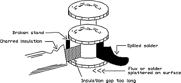
A bad solder
- The defective solder joints are cracked, pitted, cold stressed, have excessive flux or impure solder.
- For a bad solder, re-heat it and add a bit of new solder with flow to help it reflow. When very little heat is applied, it causes a dull grey solder connection instead of shiny. This type of connection is called ‘ Cold Solder Joint’. It has a high resistance and sometimes it acts as if no connection is made. Reheating a cold solder joint usually converts it into one that is acceptable.
9.9 Unsoldering Connections (De-soldering)
- A new component can not be installed unless the old one is removed. The component should be taken out without destroying the circuit board and the terminals. Thus, great care must be taken to unsolder the component.
- One of the best techniques is to use a solder sucker. It is a rubberized flexible bulb that sucks up a solder through a tube. Another type of solder sucker uses a spring-loaded piston. By using the solder sucker you can remove all of the melted solder, and then the component or the connection will be easy to remove.
- Unsoldering or de-soldering means removing a solder from a previously soldered joint. The process is useful in the replacement of a component. Along with solder sucker, two other techniques are also common, they being: Wicking and Sniffing.
- In the Wicking process a soldering wick is used. A wick is a braided wire that removes the solder by a capillary type action. The wick is heated and well-saturated with rosin, and then it placed on the top of the joint to be de-soldered. The solder flows rapidly into the rosin area due to capillary action leaving the joint to which it was previously affixed. The procedure is shown in the following figure:
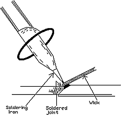
Wicking process
- First the wick is placed on the top of the solder joint to be de-soldered. Then position the iron tip on the top of the solder, due to which the iron will melt the solder. The solder will readily flow into the wick.
- Cut off the wick containing the removed solder and the wick is ready for use again. Repeat the process until all the solder is removed from the joint. The soldering wick allows for area specific control when unsoldering. You can even shape the end of the braided wire to remove the solder from small pieces.
- The wick should be about the same width as the conductor from which you are removing the solder. Do not use a soldering wick that is too wide or too narrow. Some technicians keep several sizes on hand.
- Take extreme care to ensure that the solder is not allowed to cool with the braid adhering to the work; otherwise there is a risk of damaging PCB copper tracks when you attempt to pull the braid off the joint. This technique is useful on difficult joints wherein de-soldering pumps prove unsatisfactory.
- Sniffing is one more technique used in de-soldering. Here, a ‘sniffer’, which is a rubber ball, is employed as a solder sucker. The sniffing action is nothing but the removal of solder. The following figure shows the process of sniffing:
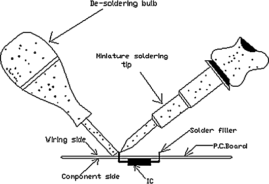
Sniffing Process
- In sniffing, air is first squeezed out of the rubber ball. The ball is depressed and the pointed end of the sniffer tube is placed next to the solder to be removed. Use the soldering iron to heat the joint and place the iron tip on the solder and not on the sniffer. Release the sniffer ball so that air enters the ball through the sniffer tube. Along with the air the molten solder is also taken into the sniffer tube.
- Ensure that all the solder is completely absorbed into the tube, then, remove the sniffer from the joint.
- A vacuum pump is also used for removal of solder. The pump uses a spring loaded plunger. The spring is cocked and the tip of the vacuum pump is held against the solder joint:
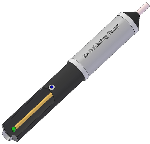
Vacuum de-soldering pump
- When the solder melts, the trigger is operated which releases the spring, creating a powerful vacuum action. Anti-static vacuum tubes are preferred as the tubes more likely to generate a static charge.
De-soldering an IC
- Multi-lead components such as integrated circuits, if they are to be removed, should be done quickly to avoid lifting of printed circuit foil conductors by excessive heat. Some specialized devices are used for this purpose.
- Use a special soldering iron tip and a spring loaded IC extractor tool:

De-soldering an IC
- The tool is placed above the IC and fixed into position. The soldering iron will heat the tip, and it is applied to all the dual-in-line IC pins. When the solder holding the IC melts, the tool takes the IC off the board.
9.10 Additional Soldering Tips
- Before you apply the soldering iron to the connection to be soldered, be sure to tin the iron. This simply means to melt the solder over the surface. The reason being that the melted solder forms a good interface. Also, make sure to tin leads or wire so that the solder is already fused with the metal. This way you do not have to hold the iron onto the surface for a long time in order to get the solder flowing and to complete your connection.
- For handling of MOSFET devices, you should take reasonable precautions, because MOSFET can be easily destroyed due to static charges. To prevent static charges from being transmitted through the board wiring to the device, it is recommended that conductive clips or conductive tape be put on the circuit board terminal.
- MOS integrated circuits are mounted on PC board after all the components have been mounted. Do not insert or remove MOS devices from test sockets with power on, to avoid transient voltages.
- Heat the parts to be soldered, not the solder. Touch the end of the solder to the parts, not the soldering iron or gun. Be careful with the amount of solder and the amount of heat. Check the component side of the board for good solders flow. SN63 is the best type of solder for electronic components.
9.11 Additional De-soldering Tips
- In the de-soldering process, when the component is replaced, they should be prevented from any mechanical shock. Devices such as semiconductors can be completely damaged, if they are dropped on the floor even from table height.
- Do not remove or replace any component when the power is on to avoid voltage or current surges.
- When the joints are stubborn, you may need to add some fresh solder or flux and then try again.
- The tools which are used for de-soldering should generate minimum amount of heat during unsoldering to prevent the damage of the base materials and the adjoining components.
- Always try to prevent damage to the copper back from the PC board, as the printed circuit board is a very expensive item.
- Do not use sharp metal objects, such as a twist drill, for removing solder from component mounting holes. Sharp objects may damage plated-through conductors.
9.12 First Aid Steps
- Soldering or de-soldering tools generate heat, because of which there is a possibility of receiving burns and electric shocks.
- The affected area should be held under tap water immediately.
- You can apply ice for some time until the burning sensation is reduced.
- Apply sterile dressing to protect against infection.
- Avoid using any lotion or ointment without medical advice.
- Finally seek professional medical advice.
9.13 Printed Circuit Board
Introduction
Printed circuitry and printed circuit boards have been defined and re-defined within the electronics industry. The following are some of the definitions:
“Printed Circuitry is a circuit in which the interconnecting wires have been replaced by conducting strips printed, etched etc. onto an insulating board. It may also include similarly formed components on the base board.”
“A printed circuit board is also called a card chassis or plate. It is an insulating board onto which a circuit has been printed.”
These definitions assume that the reader has had prior experience with point-point wire soldering. In the design process of PCB, there is a replacement of hand-soldered point-to-point wire connections with thin lines of copper. These copper lines are affixed on one or both sides of flat, rigid, glass-epoxy insulated boards through various processes including photography and etching. The board facilitates the rapid assembly of active, passive, discrete, non-discrete, and hybrid electronic components. The result is a single compact assembly where ease of assembly, maintenance and reliability are an order of magnitude better than ever before possible.
A brief overview of Design and Manufacture of Printed Circuit Board
A printed circuit board is shown in the following figure:
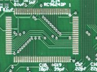
Printed circuit board
It is clearly seen that the PCB itself is a board carrying a pattern consisting of conductors and pads. The electronic components are soldered to the pads and electrically interconnected by means of the conductors. In other words a printed circuit board serves to carry and interconnect all the electronic components.
It can be easily appreciated that the use of printed circuit boards results in a more uniform and error-free product if the board pattern is accurately and consistently reproducible. The basic information required when starting to design a PCB comprises the schematic diagram and the component list together with mechanical dimensions and tolerance of the board.
A schematic is the first step because it displays and identifies the components that make up the equipment.
A schematic diagram consists of a system of graphic symbols that represents electronic, electrical, and electromechanical components. The components are connected electrically by the interconnecting lines.
In the layout stage, a sketch of the component location and the interconnections of the components are worked out. After completion of the layout, an art-master (tape-up) is generated. The taping of the artwork means the preparation of a very precise picture of the pattern, very often made on a large scale, for example, four times full size. The taping is usually carried out using self-adhesive pre-cut symbols for the various constituents of the pattern, for example solder pads, contact fingers of edge connectors, and conductors.
The artwork is subsequently reduced to actual size by photography to provide 1:1 scale negative and positive which then becomes a highly accurate tool for the manufacturing of the PC board. The reduced copy is used by the manufacturers as the master pattern. For this reason it is not possible to indicate mechanical dimensions and other relevant specifications on the artwork itself. Instead, it is necessary to prepare an engineering drawing which contains a complete specification of the printed circuit board including the mechanical dimensions, hole diameters, tolerances, and surface treatment of the boards.
During the assembly process, the components are mounted on the circuit board. To facilitate correct and easy mounting of the components, a notation is created which provides the location of the various components. The artwork for this notation is also prepared by the PCB draftsman.
Other documentation prepared from the layout and the reduced positive include fabrication, assembly, parts list and silk-screen drawing, plus whatever special manufacturing sketches or aids that might be required.
Now, let us see the manufacturing process of the PC boards. The raw material is a laminate consisting of a thin, rigid sheet of insulating material which is clad with a very thin copper foil on one or both sides. All the solder holes are drilled in accordance with the master pattern and mechanical drawing. By selectively etching all unwanted copper areas away, only those parts which form the pattern, i.e. the solder pads and the conductors, remain on the finished board. This is a subtractive process, and thus it can be easily understood that an additive process starts with an unclad base material on which the copper necessary for forming the pattern is deposited.
Whether the pattern is derived by the former or later process, its surface has to be protected to avoid oxidization of copper which would add to a serious reduction of the solderability.
An organic coating of colophony resin is given to single-sided boards. For plated-through boards, an electrolytic deposition of tin or lead/tin alloy is used. In plated-through boards, it is possible to deposit copper and tin/lead on the walls of the holes so that the holes become conductive and solderable. The plated holes serve to make a connection between conductors on opposite sides of the board.
Solder masking is a coat of epoxy resin, covering all areas of the PC board except pads which require soldering. Solder masks are increasingly being used to eliminate bridging between adjacent conductors during wave soldering.
Wave soldering is a process whereby component leads are soldered to a printed circuit board by traveling at a predetermined rate of speed through a wave of molten solder.
Types of Printed Circuit Board
Printed circuit boards come in several different types as illustrated below:

Cross-section of different types of PCB
The two main types are: Plated-through and non-plated-through boards. Plated-through boards are more expensive as compared to non-plated through. Most of the times plated-through boards are double-sided and non-plated-through are single-sided.
Plated-through boards are chiefly used in professional electronic equipment such as measuring instrument, computers and military equipment.
Non-plated-through boards are mostly used for entertainment applications such as radios, televisions, amplifiers, etc.
Methods of PCB construction
The different methods of construction of Printed Circuit Board are given in brief as follows:
Conventional
In the conventional method, a rigid PCB usually of thickness 1.6mm is used. The components are wire-leaded and they are mounted on only one side of the PCB, with all the leads through holes, soldered and clipped. Conventional circuitry is generally easier to debug and repair than Surface mount.
Surface Mount Technology (SMT) or devices (SMD)
In Surface Mount Technology, instead of inserting leaded components through holes (as in conventional method), special miniaturized components are directly attached and soldered to the printed circuit board. Holes are still needed on the PCB, but not where the component leads are attached. Surface mount circuitry is generally smaller than conventional. Surface mount is generally more suited to automated assembly than conventional.
Surface mount and conventional mix
This method employs both the conventional and the surface mount technology. In practice, most boards are a mix of surface mount and conventional components. This can have its disadvantages as the two technologies require different methods of insertion and soldering.
Double sided Laminate
In this type of method, a bare PCB laminate has tracks on both sides of the board, normally with plated-through holes connecting circuitry on the two sides together.
Double sided Component Assembly
As the name suggests, in double sided component assembly, the components are mounted on both sides of the PCB. Normally only surface mounts circuitry would be mounted on both sides of a PCB.
Multi-layer
A PCB Laminate may be manufactured with more than two layers of copper tracks by using a sandwich construction. The cost of the laminate reflects the number of layers. The extra layers may be used to route more complicated circuitry, and/or distribute the power supply more effectively.
Chip On Board (COB)
In this technology, the IC die is attached directly to a PCB and bond out wires from the IC connect directly to PCB lands. The chip is then covered with a black blob of epoxy. A technique used mostly with very high volume, cost sensitive applications, for example musical greeting cards.
Gold plated
In many cases, certain areas on a PCB may be gold plated for use as contact pads. Unless the whole PCB is gold plated before etching, this technique is limited in its application, normally to pads on the edge of a PCB, as an electrolytic plating bar must be attached to the pads and then removed part way through the PCB manufacturing process.
Flexible PCB
Flexible printed circuit boards are used when the requirement is to fit the board into specially a shaped volume. This technique is used extensively with membrane keyboards, combination connector/circuit boards, and circuit boards to fit in awkward shapes, such as. cameras. Flexible printed circuit boards can be stretched, bent, or folded as per the requirement.
Surface Mount Technology
Surface Mount Technology for construction of PCB is very popular and it has superseded the conventional through-hole mounting technology. The basic reasons for the demand of this technology are the market trend for miniaturization in electronic assembly, increased reliability, and lower manufacturing costs, improved electrical and mechanical performance.
As mentioned earlier, in this technology, the components are directly attaché and soldered to the printed circuit board. The surface-mounted components and their packing are particularly suitable for automatic assembly. The following figure shows a board constructed with surface mount technology:
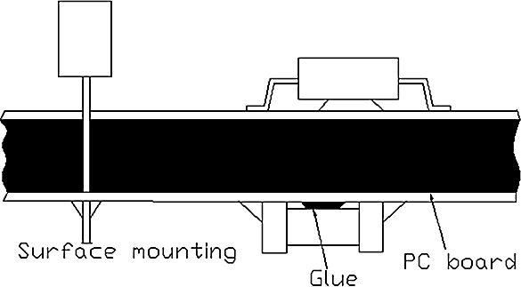
Surface Mount Technology
Here the components can be assembled on both sides of the board. A non-conductive glue or solder paste is used to attach the components to the board. For leadless components, a ceramic or glass substrate is used as a base for reflow soldering.
The surface mount components do not employ leads like resistors and capacitors have. Instead they have a metal interface that is used for soldering. The following figure shows a comparison of a conventional resistor with a surface mount resistor:

A conventional resistor with a surface mount resistor
In this technology, the removed component is never replaced back in the circuit. A new component is used for replacement. In order to handle surface mount components, a vacuum parts holder can be used. Also, there is a special solder cream that can be used for soldering onto circuit boards. 60/ 40 type of solder is avoided. The amount of temperature required to melt this solder is surely enough to destroy the component. Also a solder with acid flux is never used in electronics.
Surface Mount Devices
- The components used in surface mount technology are abbreviated as SMD, Surface Mount Devices. SMDs are designed with soldering pads or short leads and are much smaller than comparable leaded components.
- The leads of the conventional components are inserted into the holes, while SMDs are directly attached to the printed circuit board and then soldered.
- Resistors, ceramic capacitors and discrete semiconductors represent 80 percent of the total available SMDs. Normally, in the SMDs, the cubic shape prevails over the cylindrical version, as the latter can only have two pins, thus being exclusively suitable for resistors, capacitors and diodes.
- Because of certain reasons, if the SMD package is not possible, then the DIP package can also be converted to surface mountable versions by bending the leads. Depending upon the component, there can be different types of lead styles, with which SMDs are constructed. Lead Pitch is also an important factor for SMDs, which is measured from center-to-center of leads and in not the air gap between the leads. The following table shows commonly used lead styles:
Commonly Used Lead Styles
| Type of Lead Style | Figure | Components |
|---|---|---|
| Gull Wing: metal lead that bends down and away |
 |
SOIC (Small Outline Integrated Circuit) QFP (Quad Flat Pack) TSOP |
| J-lead: metal lead that bends down and underneath a component in the shape of letter J |
 |
PLCC (Plastic Leaded Chip Carriers) SOD (Small Outline Diode) |
| Ball: metal lead in shape of a ball |
 |
BGA (Ball Grid Array) CHIP SCALE FLIP CHIP (Bump) |
| Metallised Terminations: metal leads are terminated |
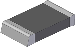 |
Capacitors Resistors Ferrites |
- In order to protect the SMDs during transport, proper packaging is required. The various packaging methods to provide proper feeder to receive the components are trays, tubes, and reel and bulk feed cassettes.
- In SMT, the size of the components is defined in code which may be stated in inches or in the metric system.
9.14 Troubleshooting of Surface Mounted PCBs
Troubleshooting of faulty SMT assemblies usually require removal and replacement of components. The need for troubleshooting arises when there are damaged pads and tracks due to inappropriate or careless component removal practices. These damages are mostly due to inadequate training of the repair workers in properly understanding and handling the SMT PCBs.
The simplest method to remove the faulty components is cutting all leads. Each leg is cut carefully and then the component is taken off. Each joint is then melted with a fine tip, temperature controlled soldering iron and remaining IC legs are removed with tweezers. The tweezer uses the squeezing action to remove a variety of parts.
After allowing a cool down period, excess solder is removed with a de-soldering braid. This method does not require any tool and special workstation; hence it is cheap. But it can damage the components while cutting, thus in turn damaging the PCB substrate and copper pads. Also, soldering the replacement component in position using a soldering iron requires processing one lead at a time. Hence it is also time consuming.
In order to rework the SMT PCBs, two basic heating methods are introduced. These methods are conductive and convective methods. Let us understand these methods:
Conductive Method
- This method uses a heated tool that contacts the solder joint to effect reflow. The soldering tools are provided with the tips designed to heat all the component’s leads. Their electrodes come in contact with component legs and hold them flat to the copper pads on the PCB.
- Sometimes a controlled pulse of current is also used which passes through the electrode which heats the component leads. This melts the solder on the joints and the built-in vacuum pick-up lifts up the component from the surface.
- The technique enables all the leads to cool down rapidly after the soldering operation and so allows the leads to be held in position while the solder solidifies. The conductive does not heat the component body and it is very fast and repeatable.
- It is also very good for replacement as the electrodes will hold the legs flat to the pads during the solder reflow, while the alignment and positioning is ensured with microscope. The process is a little expensive.
Convective Method
- It is known as hot gas soldering where a hot gas or hot air is used as the heat transfer medium. The hot gas is swept over the leads until full reflow is achieved, after which a part is lifted with a tweezer.
- Small parts such as chips, transistors, SIOC and flat packs can be removed with a single point nozzle. With longer components, a component specific nozzle is fitted to the hand piece and brought around the part to remove the surface mounted devices.
- The vacuum pick-up lifts up the component after reflow. Sometimes infra-red radiation is also used for re-flow of the solder joints. The process takes a longer time for removal as compared to conductive method.
Removal of SMDs
The following steps should be performed for removal of a component using a hot gas machine:
- Apply a small amount of liquid flux to the joint.
- Chose the correct head to suit the component.
- Keep the PCB in place and activate the gas flow to reflow the solder on every joint. A Video Display Unit or microscope can be used.
- If the component has been bonded with an adhesive, rotate the head to shear the bond.
- Remove the component with the vacuum pick-up and allow the PCB to cool.
- Remove any remaining solder with the help of a de-soldering braid.
- Allow a further cool down period and lastly inspect the pads to ensure that they are not damaged.
Replacement of SMD
The following procedure is followed for replacement of components:
- The new component is inspected to ensure that the legs are not bent or distorted.
- A thin film of flux is lightly applied to the pads.
- The component is then placed into the head of the hot gas machine and carefully lined up to the PCB.
- The components are lifted away from the board, until the legs are just clear of the pads. Then the gas flow is initiated. The applied gas heats up the legs and the solder on the pads.
- At the time when the solder is flowing, the legs of the components are made to sit between the fingers of the tape and hence are central over the pads.
- Make sure that the solder flows correctly around each leg, until then the gas is allowed to flow.
- Stop the flow of the gas when the solder is distributed evenly around the leg and allow the board to cool at least for one minute to avoid disturbing the joints.
- Remove the PCB from the machine and then carefully remove the Solder Quick tape and clean all the excess flux from the joints.
- Inspect all joints with magnifier to ensure correct reflow.
- Clean the PCB with isopropyl alcohol in the aerosol form to ensure penetration of the solvent under the component to wash out any flux. The area can then be brushed to remove all traces of flux.
9.15 Testing and Troubleshooting with ATE
The main objective for testing and troubleshooting of a printed circuit board is to ensure that the components which might have been damaged during assembly, including mass soldering are identified so that they can be replaced before the board reaches the functional test stage. The use of Automatic Test Equipment (ATE) is very common for the purpose. Automatic test equipment is primarily intended to test assembled boards.
Automatic Test Equipment (ATE)
- The automatic test equipment is popular because of board complexity and the growing problem of finding qualified personnel to perform the testing and troubleshooting. With this the board is tested without delay and with fewer complications. The test equipment usually contains a guard system. This guard system functions to isolate any components from all the other components on the board.
- In these types of equipment, there is a test program written for a particular type of board. The components are tested in sequence according to this test program. The designations of possible defective components are automatically printed on paper so that such components can be identified and replaced.
- ATE can also test the pattern itself for short circuit and interruptions. However, near shorts and near opens can not be detected by ATE.
ATE with movable base plate
Here the test equipment and the assembled board are connected via a bed of nails, on which the board is placed:
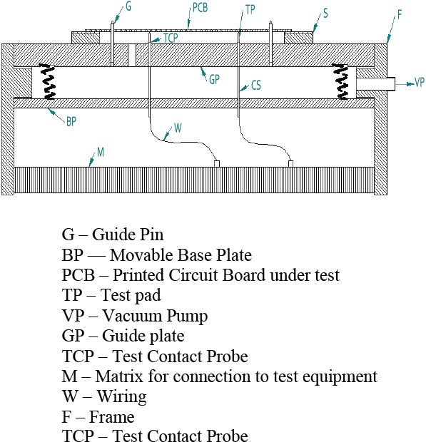
Cross section of ATE with movable base plate
- The base plate carries the number of fixed and movable test contact probes. The movable probes are controlled by a fixed guide plate. By raising the base plate, the ATE makes the contact probe upwards to make contact with selected test points.
- There is a retainer spring inside which determines the contact pressure inside the test contact probe. The base plate can be raised with a vacuum pump. The pump evacuates the chamber between the guide plate and the base plate.
- In order to maintain the vacuum, all leakages must be reasonably small. The board is therefore sealed by a gasket along the board edges. The larger holes in the boards are sealed by suitably shaped gaskets glued to the guide plate. For bare-board testing, a plastic sheet placed on the top side of the board can seal the smaller holes but larger holes must still be sealed by gaskets.
- The board must be oriented correctly with respect to the test contact probes. The simplest way is to use the board’s tooling holes and to mount guide pins at the right places in the guide plate.
ATE with Fixed base plate
The test contact probes are mounted in the fixed base plate:
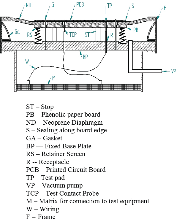
Cross section of ATE with fixed base plate
- Instead of a fixed guide plate, a Neoprene diaphragm is used. The center part of the diaphragm is made rigid by a phenolic paper board which is attached to the under side of the diaphragm.
- Since the phenolic paper is somewhat smaller than the diaphragm, the diaphragm can move downward when the vacuum activates the fixture (the bed of nails). Because of the vacuum, the board under test follows the diaphragm so that the probe tips hit the test pads.
Advantages of Fixed base plate
- The fixed base plate does not create sealing problems, because the vacuum created, is higher.
- The test contact probes are inserted into wired receptacles mounted in the base plate, so that they are readily removed for cleaning or replacement.
- The wiring from the receptacle does not move when the fixture is activated. Hence, there is breakage or damage to the wiring.
Guarding Technique
Guarding technique is a method used by most ATE systems. In this technique, it is possible to measure a component soldered in place on the board, without having to interrupt conductors or to de-solder the components. The PCB pattern can also be tested for interruption and short circuit, even if all the components have been soldered in place.
The guarding technique implies the use of various methods of connecting the equipment, depending upon the type of the component and the adjacent circuitry.
To use the guarding technique, it is necessary that one should have the knowledge of establishing the necessary test points in the form of special test pads, and various design rules.
The test engineer marks the necessary test points on the schematic diagram, which (test points) in the layout stage are treated in the same way as all other components.
Establishing Test Points
- To auto-test a printed circuit board, the ATE systems must establish electrical contact to the terminals of each component. Since the components will necessarily be connected with each other in various configurations, they have a number of points in common.
- In schematic diagram, a common point is represented by a conductor line interconnecting one side of a number of components. This point is called a nodal point. The following figure shows a nodal point:

Test points for testing components (a): Section of a schematic diagram

Test points for testing components
(b): redrawn schematic diagram with indication of nodal points (NP)
- With the help of a nodal point any component can be accessible for testing. In the board, the nodal point occurs as a conductor which connects a number of pads with each other. The test engineer has to indicate the nodal points on the schematic diagram, and to treat the points as a type of component to be placed on the solder side of the board during the layout phase. Only one test point, in the form of a test pad, should be connected with the conductor that represents the nodal point.
- If the board pattern is very dense, it is difficult to make room for all test pads. Also, the test equipment can have a limited capacity that restricts the number of test points, e.g. to 1000. In such cases, it is necessary to reduce the number of test pads. The test engineer can divide the test points into two or more categories, such as absolutely necessary points and desirable but dispensable test points.
What is a Test pad?
The basic function of the test pad is to serve as contact points for the test probe tips. The use of test pads implies an immediate advantage by defining the various test points very precisely. Figure 9.26 shows a test pad.
The test pads are not drilled; hence they do not increase the manufacturing cost. An important advantage of using special test pads is that changes in the circuitry do not necessarily result in changes to the drilling pattern of the base and guide plate/diaphragm. In many cases, the components are moved a little, but the test pads remain untouched.
Test for short circuit between conductors
- In the test equipment, it is possible to determine the short circuits between the conductors with the help of resistance measurement. Conductors exhibiting short circuits are indicated by a printout of their numbers so that they can be identified:
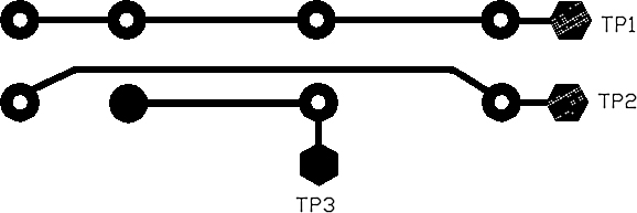
Test of short circuit between conductors
- As shown in the above figure, it is not necessary to connect more than one test point to each conductor in order to perform the test. The test points are therefore identical with the test points for components.
- When there is large distance between conductors and the remaining parts of the pattern, the probability of short circuits in the form of etching faults and solder bridging is practically zero. In such cases, there is no need of testing for short circuits, but for the sake of component testing, a test pad should be connected to the conductor at the nodal point.
Test for interruptions of conductors
- Interrupted conductors are caused by mishaps during the pattern imaging. In case of bare-copper boards, voids in the etch resist can allow the copper to be etched, and in case of plated-through boards the plating resist perhaps was not removed completely, so that the tin/lead layer protecting the conductors against etching contained voids.
- Other reasons can be the overlooking of minor faults in the master film or dry film resist, such as an unfortunately located pinhole in the photosensitive layer. Also scratches in the plated tin/lead layer, which act as etching resist, can cause an etching of short length of conductor.
- Whether a conductor is interrupted or not can be checked by measuring the resistance between its two ends. Sometimes it is difficult for the test engineer to decide whether it is a component fault or a pattern fault. The result is often that the engineer chooses to replace the component. In such cases the interruption of the conductors can not be seen immediately. It can be a nearly invisible track or the fault can be hidden under a component. Therefore, it is considered safer to establish direct test access to the conductors using a test point at each conductor end, shown below:

Test for interrupt of conductors
- In this way, all partial conductor lengths including possible via holes are checked. The resistance will normally be in the range of milliohm, i.e. practically zero. Long conductors are more exposed to interruption than short conductors.
Placing of the Test Points
All the test pads must be placed on the solder side of the board. Conductors act as connecting lines between the solder pads. The conductors are accessible on the component side through the plated-through holes from the solder side. In case of a double-sided non-plated through board, there will be either a component lead, a piece of wire, or an eyelet soldered to both sides of the board. It is therefore necessary to achieve contact with conductors on the component side by connecting the test pads to the solder pads on the solder side. There is a set of design rules, which will aid the PCB test engineer in deciding where to place the test points physically:
- A test pad is connected to each necessary test point (nodal point). The location of the connection is of minor importance, but in the case of interrupted conductors, the test pads are connected to the extreme end of the conductors.
- When the space available permits, the test pad is connected to every desirable but dispensable test point.
- In case of a power bus, two test pads are connected. The reason is that a common terminal for both power and test signals can give misleading results during the test.
- A test pad should be connected to a functional by unused IC terminals, such as a gate output. A short-circuited and unused gate can adversely affect other parts of the IC. It is therefore recommended to include such unused components in the test.
Contact Problems with ATE
While using Automatic Test Equipment, the test contact probes are used to make contact with the selected test points. In practice, there can be contact problems, particularly in the case of assembled boards. Usually solder pads are commonly used as test points. The dimensions of the solder pad are very small because of which it is difficult for the probe to hit the pad. The common problems occurring while making contact are:
- Many a time, the contact probe misses the solder pad. It happens when the component lead soldered to the pad is a little too long because of which it might have bent upwards slightly. The following figure shows this type of problem:
Deflection of test contact probe: (a)
- Another type of fault in contact can be the probe tip’s short circuiting the two component leads:
Deflection of test contact probe: (b)
When the two component leads are cut a little too long and bent towards each other, there are chances that the contact probe touches both the leads. Sometimes the tip of the probe is so wide that the tip itself causes short circuit.
Prevention of Contact Problems
A printed circuit board should be designed to permit automatic testing without any contact problems. In order to prevent the contact problems discussed above, first the test points are selected and then special test pads are connected to these test points:
Use of special test pad
These test pads are used to serve as contact points for the test probe tips.
9.16 Summary
Soldering is an alloying process between two metals. Most of the solders used today are 60/40 type, i.e., 60 percent tin and 40 percent lead. A better is of 63/37 variety which has 63 percent tin and 37 percent lead.
Soldering iron, solder pencil, solder gun and strippers are the soldering tools. A solder is an alloy of lead and tin which is used for the purpose of joining together two or more metals.
A flux is used to scrub away the microscopic film of oxides on the surfaces of metals to be soldered. Flux is applied before or during soldering.
The component to be soldered must be properly formed and fit into the circuit in which they are to be installed. The component forming procedure ensures some important steps that are to be followed, to make the component ready for soldering.
Wicking and Sniffing are the two techniques used in the de-soldering process.
In general, if any system is maintained properly, the failure rate of the system decreases, as a consequence the reliability of the system increases. In this chapter the basic requirement of maintenance is explained. In any organization, it is considered essential to establish a sound policy of maintenance to ensure continuity of service from the equipment.
This chapter provides information on the various groups in a maintenance organization and how they operate.
Learning objectives
- Understand need of maintenance
- Know the structure of maintenance
- Study of Preventive maintenance
- Study of maintenance policy
- Study of maintenance organization
- Understand safety aspects and quality of operation
10.1 Do we need maintenance?
- The answer is obviously yes!!! In general, to get the desired results out of any system, the system is designed in such a way as to have maximum protection against errors. But still, many a time, the system fails to operate normally and starts giving undesired results. When the results are not up to the mark, then there exists a conflict between the system performance and the user expectations.
- Why does this happen? This may be due to the faults which are arising in any of the equipment in the system. There can be various causes for these faults. One of the major causes is low maintenance.
- The question of maintenance arises, when the equipment does not perform according to its specifications. The basic motive of the maintenance is to prolong the life of equipment and increase Mean Time Between Failure (MTBF).
- Maintenance in an organization is the upkeep, repair, renewal and replacement of worn, damaged, or obsolete parts of equipment. A good maintenance practice ensures a maximum operating time of the equipment causing low maintenance cost. With all the above things in mind we can say, yes, we need maintenance!!
10.2 Types of Maintenance
Depending upon when the maintenance comes into picture, it can be classified into the following categories:
- Corrective Maintenance
- Improvement Maintenance
- Preventive Maintenance

Structure of maintenance
Corrective Maintenance:
- It is also known as Breakdown Maintenance. We are all aware of breakdown maintenance activities. In fact most of the awareness in the minds of the technician about maintenance itself is centered on how quickly a breakdown is attended.
- Corrective maintenance means that the action is taken only when the need for it becomes obvious, and therefore gives no assurance that a major breakdown will not occur.
- It is also known as Remedial Maintenance. It consists of efforts to restore facilities and equipment to an acceptable operating condition after a breakdown has occurred. Some maintenance organizations provide standby equipment so that breakdowns do not stop the process and equipment can be repaired at scheduled times.
Improvement Maintenance
- Improvement maintenance is an attempt to reduce the need for maintenance by changing, redesigning and retrofitting a machine to overcome some problems in an existing machine.
- With this type of maintenance the overall performance of the system is improved. It includes elimination of failures that requires maintenance.
Preventive Maintenance
- Preventive maintenance means all actions intended to keep equipment in good operating condition and avoid future failure. A good preventive maintenance program is the heart of effective maintenance. It is an activity designed to prevent wear and tear or sudden failure of equipment. It involves a policy of replacement of components of a system before the component actually fails. Let’s look at the advantages of preventive maintenance.
Advantages of Preventive Maintenance
- Preventive maintenance implies frequent inspection to detect minor faults and the early correction of them, supplemented by periodic overhauling in accordance with a plan so that a possibility of major breakdown is almost entirely eliminated.
- An equipment in good working order subjected to a regular inspection and adjustments will continue to produce quality products for a longer period than otherwise. An efficiently managed preventive maintenance system improves working conditions and therefore it has a great importance amongst all types of maintenance.
- For continued, good service of equipment, the equipment has to be in a good working condition. If this is accepted, it becomes obvious that the preventive maintenance system guarantees the continued good working of equipment.
- In fact, preventive maintenance occupies the same position with regard to equipment as preventive medicine does with regard to public health. If preventive maintenance is performed at predetermined periods and coordinated with the production schedules, the quantum of production will automatically increase.
- A branch of preventive maintenance called “Predictive Maintenance” applies sensors and analysis of technical data to determine when the performance of a piece of equipment is about to degrade or when it is about to break down. It is intended to prevent breakdown. Predictive Maintenance is a program of periodically monitoring equipment and tracking certain measures of its performance.
- Predictive Maintenance is more feasible today because of technology that is available for equipment surveillance and diagnosis of problems while the machines are still running. The condition of equipment can be monitored by several means. Critical monitor points on the equipment are identified. Sensors may be installed or periodic readings may be taken with portable units to measure the temperature or vibrations. Vibration sensors and ultrasonic sensors are used to feed data into a computer for analysis.
- A program of this type prevents unplanned downtime that disrupts production schedules, creates an idle work force and degrades customer service. Equipment is out of service for a very short duration because much of the diagnostic work has already been done and the necessary parts and people are available.
Preventive Maintenance Records
In order to measure the effectiveness of a preventive maintenance program, a statistical feedback is required. The equipment failure and repair history provides valuable information for analysis to see if PM is effective, and if not what steps are to be taken to make it more effective. All the work done on the equipment should be recorded in the history card.
The history card should maintain the number and duration of each repair, name of the person who serviced the equipment, and any parts replaced. The history cards are generally prepared from the maintenance work order.
The preventive maintenance record should include:
- Name of the equipment
- Identification number of the equipment
- Location
- Preventive maintenance done
- Next preventive maintenance due
- Last preventive maintenance done
- Spare parts required
- Equipment required
10.3 Aims of Maintenance
- Maintenance aims primarily to keep in efficient operating condition the productive plant and equipment, their auxiliaries, general engineering services, material handling units and so on.
- Maintenance also aims at keeping to the minimum possible level down-time of equipment so as to ensure their maximum availability for production. Good maintenance leads to higher output through lower down-time of equipment, better quality of products through improved efficiency and a lower unit cost because of less breakdown expenses.
- In short, the objectives of maintenance are twofold to keep the organization in operating condition and to arrest depreciation and forestall obsolescence.
10.4 Advantages of Preventive Maintenance
- Management control over downtime: Management has a control over planned maintenance activity and can pre-act instead of react.
- Reduced overtime: The maintenance work is done when convenient to both the users and staff. Hence overtime is reduced.
- Standardized procedures: Management designs some standardized procedures for the effective maintenance.
- Better distributed workloads: The preventive maintenance ensures all the available resources in manpower as well as equipment.
- Improved safety: Preventive maintenance provides constant monitoring over the system due to which dangerous situations can be avoided.
10.5 Importance of Sound Maintenance Management
Maintenance efforts must be managed effectively to keep any type of interference to a minimum level. Operating maintenance costs money, so it should be planned and controlled just as any other department should be.
Maintenance activities affect equipment return on investment because they represent an expense and because downtime of maintenance may cause missed deliveries. Maintenance done in an effective way affects the operation of the equipment, which directly affects the quality of the system’s output. Maintenance also influences return on investment because it affects the economic lifetime and salvage value of the equipment. The objectives of the maintenance management include:
- Minimizing the loss of productive time and cost by ensuring proper functioning of the equipment.
- Minimizing the loss of productive time and cost because of maintenance efforts.
- Efficient use of maintenance personnel and equipment.
- Preserving the company’s investment and prolonging the life of assets to increase the time over which investment provides service.
10.6 Maintenance Policy
In any organization, whenever new equipment is purchased or a replacement of an existing worn out equipment is planned, the maintenance department has an important role to play. However, the right selection of equipment holds the key to forming a good maintenance policy. The maintenance policy must consider the following important points for successful continued maintenance:
- Choosing the right equipment
- Selecting a supplier
- Ordering spares and
- Warranty
Let us address all these points one by one.
Choosing the right equipment
- The user must be sure that he is buying equipment that he really needs. He should be able to select the equipment which will best suit the economic as well as the technical range.
- The technology changes everyday. So, keep track of changing technologies. Some technologies are progressing so rapidly that it has made the job of selection difficult.
- For choosing the right equipment, always look for performance and features. There are many new types of equipment that have user friendly features that make measurement and operations easier. But this should not affect the overall performance. The difference between performance and features must be clearly understood.
- The person, who is selecting the equipment, should have prior knowledge about the exact requirement and the current equipment available in the market which fulfills the requirement. Usually, the concerned maintenance engineer does this job. The engineer should contact the maintenance department before placing any order.
- The purchase order should be placed properly. The person, who is ordering the purchase, should go through the purchase contract thoroughly. The purchase order should insist on complete documentation, warranty period, free service period, training in operation as well as in maintenance, installation, a discount if given.
Selecting a supplier
- Ensure that the supplier has the proper infrastructure to make the product. The purchase function has what is known as the Vendor rating in which the capacity of the supplier to manufacture as per certain standards is asserted and is given a rating. This will ensure reliability in the supply.
- A branded supplier will guarantee a basic quality standard and very little inspection required. On the other hand, a smaller supplier may supply the equipment as per the purchase order, but may have problems in long term reliability. We must assess a supplier before we place an order with them.
- For special purpose machines we must remember that making a proposal is a time consuming and costly affair. Do not ask for proposals from too many suppliers as it involves a lot of time to evaluate the proposals.
- The purchase order for a special purpose machine should be the culmination of countless discussions with a comprehensive statement of the work to be done, engineering and machine acceptance terms, payment terms, installation, documentation, training, etc.
- If the system can be divided into many parts or functions, then it is better to break up the cost of each function so that in case of subsequent modification, the implications on the cost can be worked out.
- For imported equipment, the major issue can be the distance between the user and the manufacturer. Spares have to be stocked in larger quantity. Make sure that the document and the manuals are in the English language or in local language.
Ordering Spares
- The components in electronic equipment are manufactured by several specialized companies. The equipment manufacturer gets the components from these suppliers of components. Sometimes the components are purchased from a trading agency.
- While ordering spares, the person in charge, should have sound knowledge of the component number, name of the component and its description, name of the company, and so on.
- The manufacturers have their specialized way of coding for the component number which is denoted by the component number. The component number specifies the assembly reference and the component circuit reference.
- Many components are selectable, for example the equipment manufacturer selects the components from a batch supplied by the component manufacturer that meets the manufacturer’s specifications.
- In case of imported equipment, spares may not be available in the local market and will have to be imported. This takes considerable time and money. So, it advisable that a list of spares is bought with the instrument to avoid downtime. A set of essential spares can be kept in stock for 2 to 3 years. This requires some extra maintenance.
Warranty
- The type of the warranty, conditions for warranty, and warranty period is all decided by the manufacturer of the equipment. Depending upon the type of the component and its future use, all the above factors are decided by the manufacturer.
- Generally, the manufacturer asks the buyer to pay for the repair, in case the failure is caused by misuse, improper handling, etc.
- The documents of the warranty are to be preserved by the user for future use. Usually the warranty period begins from the day of purchase.
10.7 Maintenance Organization
Any system or equipment, for ensuring its desired way of operation needs proper maintenance. A plant or facility which depends for its operation on particular equipment needs to have a proper organization for the maintenance of its assets.
A maintenance organization would have many departments in it. These departments have the authority to take care of many activities and provide smooth running of the facility. Generally, the departments in the organization streamline their work. To do this, they can have the following groups:
- Engineering Group
- Equipment Repair and Maintenance Group
- Central Services Group
- Construction or Civil Engineering group and
- General Maintenance Group
However, the management of these groups and departments depends on the company. It may vary from company to company depending upon the exact requirement. The functions of each group are given below:
Engineering Group
- Equipment installation
- Equipment inspection
- Maintenance, stores and purchase
- Estimating and costing
Equipment Repair and Maintenance Group
- Breakdown maintenance of electrical/ electronics/mechanical equipment
- Preventive maintenance
- Computer and network maintenance
Central Services Group
- Air conditioning
- Water limes, steam lines, air/gas lines
- Pollution monitoring and control
- Electrical substation and generating plants
- Protection against fire
- Vehicle maintenance
Construction or Civil Engineering group
- Building maintenance
- Modifications in civil works
- Addition of new construction works
- Sanitary maintenance
- Horticulture.
General Maintenance Group
- Furniture maintenance
- Billing
- Cleaning
- Transport Service, etc
10.8 Maintenance Manuals
When the equipment is sold, the manufacturers usually supply the maintenance manual which contains the following information:
- Component description, their specifications and rating
- Description of block diagram
- Description of assembly of the equipment
- Description of dismantling of the equipment
- List of test instruments and special tools
- Test procedures
- Test points with DC voltages and operating waveforms
- Fault conditions of the component and their probable causes
- Safety procedures to be observed while carrying out the tests, and while dismantling
However, the information carried in the manual may vary from manufacturer to manufacturer depending upon the type of the equipment.
The user manual provides necessary information for operating the equipment, start-up and shut down instructions, general design concepts, specification and installation procedures. Operator level maintenance instructions including preventive maintenance manuals are useful for preliminary diagnostics establishing preventive maintenance schedules.
10.9 Safety Aspects
Introduction
Safety is the first essential requirement a technician should learn before he starts working on equipment. Safety is an attitude, a form of mind for the technician. Safe working habits can not be brought or manufactured, they are learnt through practice.
The person who is handling equipment, or troubleshooting any system, the most important thing which he has to keep in mind, is safety. Personal safety should be given the highest preference, and when following the safety rules properly, gives the best result for troubleshooting. One should practice safe working procedures at all time while working on systems.
Personal Safety
- While handling electronic equipment, there can be many hazardous situations, which should be avoided by following some essential precautions for your personal safety. The safety precautions depend upon the equipment/system you are working on. But, there is a general set of precautions which should be followed to be safe from dangers.
- The main danger in servicing electronic equipment can be the hazard of electric shock. The equipment is usually sourced from a power supply of 220 V. That can be a real danger if your body becomes a part of the electrical circuit. The human body’s electrical resistance is quite low, and the amount of current flowing through the body depends upon the body’s electrical resistance.
- Now-a-day most modern equipment are solid state devices and they work on low voltages. But motors operate on higher voltages, also as said above; power supply also has higher voltage. You must be cautious while touching any component or part of the equipment during troubleshooting. Also you have to be careful about your clothes while servicing.
- Electric shock hazard is particularly present when servicing TV, computer, microwave equipment, video monitors, SMPS, electronic flash unit, power tools, and so forth.
- Use an insulated rubber mat which should be thick enough so that your feet will be separated from ground. The rubber mat should be dry and away from water. Use insulated hand tools.
- Never touch a hot AC line when working with mains-operated equipment. It is advisable to keep one hand in your pocket when around the high voltage system.
- Do not forget to unplug the equipment. Perform as many tests as possible with power off. Turn on the equipment only when the measurements are to be taken, assuring that there is no unwanted short circuit.
- Always keep your fingers away from any moving part and mechanisms. Use some insulated tool or protective gloves. Do not wear any jewellery that could contact some mechanism or get caught in moving parts. They may conduct current.
- The lasers from CD/DVD-ROM drives, CD/DVD players, optical data storage, etc. can affect skin and vision. Those who have potential allergies for skin rashes or vision problems should be careful of these hazards.
- Make sure that the equipment you are servicing has a ground to ground chassis. It is advisable that you know the equipment thoroughly. Many types of equipment have metal chassis as ground return. Sometimes the chassis may be electrically live with respect to the earth ground of the AC line. Do not assume that chassis is suitable ground for the test equipment.
- Try to avoid short cuts. Do not totally rely on the user’s information. Always check out what the user is saying by taking readings or doing preliminary checks. So never assume anything without checking.
- Always keep one more person with you while servicing. Do not work alone. The other person may be useful in case of an emergency. Do not work forcibly or when you are tired. The effective time of troubleshooting will be reduced. Negligence due to tiredness may prove dangerous.
Accident
An accident is an unplanned and unexpected event which is likely to cause an injury. Proper diagnosis helps in preventing future accidents. Accidents cause loss of man power, work material and money. The main causes of accident at workstations are:
- Ignorance of the work, equipment and tools
- Curiosity, not knowing enough about the equipment
- Over confidence
- Over time
- Bad environment
- Improper method of work
- Less interest in work
- Use of incorrect tools
- Carelessness
- Poor working conditions
- Lack of cleanliness
- Bad planning
- Lack of discipline
- Dangerous materials with which to work
Clothing and House Keeping
- Wear clothing suited for the job. Wear shoes with thick soles. If heavy electrical work is to be done, wear safety shoes.
- Do not wear rings, watches, bracelets, or other jewellery that could get caught in moving parts.
- Do not wear neckties or loose clothing of any kind.
- The sleeves of the shirt must be short or rolled above the elbows.
- Keep the floor free from oil, grease, or any other liquid. Clean up spilled liquid immediately as it can cause a slipping hazard.
- Do not leave tools on the work table when not in use.
Fire Prevention
A fire has a small beginning and builds to leave nothing behind it. Fire prevention is always better than fire fighting. Highly flammable materials should be stored separately in another room. Only a minimum quantity of such materials should be allowed into the workplace at any time.
Causes of Fire
Loose connections of electric wires
Smoking
Overloading on electric wires
Short circuiting of electrical wires
Careless storing of flammable materials
Types of Fire
Fire due to electricity, Fire due to oil
Fire due to gas, Fire due to wood
Fire due to cotton, Fire due to chemicals
Fire due to flammable materials
Fire Fighting Equipment
Fire extinguisher, Fire brigade
Buckets full of water, buckets full of sand
Canvas sheets
Immediate actions when fire takes place
Inform higher authority of the workshop
Inform other persons in the workshop and ask them to leave the place
Inform the fire brigade
Use fire extinguisher
Switch off the main line
Immediately take away valuable materials
Don’t throw water on electric wires
First Aid
The accident may occur at any time during servicing. It is necessary to have first aid facilities at the workplace, so that preliminary treatment may be given to the person before reaching the doctor.
Duties of First-Aider
The main duties of the first aider are as follows:
To reach as soon as possible the first aid box at the place where the accident occurs
To give necessary treatment to the patient
To bring the patient to the first aid room for further treatment
To call the doctor as soon as possible or to take the patient to the hospital
To have full sympathy with the patient
First Aid Materials
Tincher iodine, Tincher Benzone, Spirit Ammonia,
Detol, Burnol, Plasters, Bandages, Cotton,
Knife, Scissors, Measuring glass, Antiseptic cream
Eye washing glass, Dropper, Safety Pin,
Stretcher, and necessary capsules and tablets, etc. are required.
Quality of operation
- The efficiency and final output of troubleshooting depend, to some extent, upon the quality of the operation of the equipment. The quality of work in repair and servicing, are important issues to be considered.
- As said earlier, the equipment must be turned off when removing or replacing any part and it should be turned on only while taking readings.
- Always follow the specified steps which are given in the service manual. Equipment has its own way of troubleshooting. So always keep track of the steps prescribed in the manual.
- Before troubleshooting, clean the area. The area where the equipment to be serviced, should be free from paper pieces, wires, any conducting or insulating material, solder, dust, sand particles, and so on.
- Always carry a small plastic box with you. This will help you in collecting small screws, nuts, and washers while opening equipment. Unscrew all the screws carefully so that they do not fall into the equipment, which may cause a short circuit. If it does happen, the screw should be removed immediately.
- Use minimum force while pulling the circuit board from the connectors; otherwise it may cause damage to the connectors as well as the circuit board components. Some small components may break due to a greater amount of force. Use special circuit board pullers, if available, for this purpose.
- Think twice before you apply your ideas. Make a habit of noting down the mistakes done in the past on a sheet of paper and carry that paper with you so that the mistakes will not be repeated again.
- If you are maintaining good quality in your work and employ good working habits, the process of troubleshooting will not be a troublesome job and will be successful.
10.10 Summary
The basic motive of maintenance is to prolong the life of equipment and increase Mean Time Between Failure (MTBF).
Corrective Maintenance, Improvement Maintenance, Preventive Maintenance are the three types of maintenance.
A maintenance organization has many departments in it, such as: Engineering Group, Equipment Repair and Maintenance Group, Central Services Group, Construction or Civil Engineering Group, and General Maintenance Group. All these departments are assigned to their related areas and they work separately under one organization.
Safety aspects involve personal safety. The person handling high power equipment should be cautious of shock hazards and aware of proper safety procedures.
Questions
Section 1 (Covers chapters 1 and 2)
Single Line or Multiple Choice Questions
- Define troubleshooting?
- Troubleshooting a system means to:
- Isolate the defective circuit
- Find the faulty transistor
- List any six pieces of test equipment that is used in troubleshooting of electronic systems.
- Arrange the following components in the proper order of their occurrence of failure:
- Active Devices
- Passive Devices
- Mechanical and electromechanical devices
- Electrolytic capacitors
- Amplifiers, rectifiers
- Choose the correct sentence from below:
- In the convergent path technique of troubleshooting, there are two or more input lines which feed a circuit block.
- In Divergent Path technique, there are two or more input lines which feed a circuit block.
- In Switching Path technique, the switch-able parts in the circuit under test are faulty.
- Match the following pairs:
- Equipment —-Terminal board with component parts
- Assembly —- Radio Transmitter
- Element —- Resistor
- Component —- Filament
- System —- Television
- After looking for obvious defects and considering the symptoms, the first actual measurement with the test equipment should be, to:
- Check the condition of the ON/OFF switch
- Measure the power supply voltage
- During the Infant Mortality Period, the bathtub curve shows an increasing failure rate. Choose the correct answer from below:
- The statement is correct
- The statement is incorrect
- List any five types of equipment failure.
- Read the following statements carefully and choose the correct answer:
- Early Failures are also known as Infant Failures
- Wear-out Failures occur during useful life of a system
- Random Failures occur due to ageing of the component or system.
- Statements I and II are correct
- Only statement I is correct
- Only statement II is correct
- Statements II and III are correct
- Write the formulae for following terms:
- Failure rate
- MTTF
- MTBF
- If there are 5 transistors under test and their time to failure are 400, 500, 750, 300 and 600 hours. The Mean Time To Failure is:
- 600 hours
- 510 hours
- 310 hours
- 750 hours
Descriptive Questions
- Describe some common troubleshooting techniques.
- List the causes of failure.
Section 2 (Covers chapters 3 and 4)
Single Line or Multiple Choice Questions
- Which of the following is less susceptible to extraneous noise?
- Digital Multi-meter
- Analog Multi-meter
- Which one of the following are preferable if very small changes in a level need to be determined?
- Digital Multi-meter
- Analog Multi-meter
- When the peak to peak voltage is calculated from the waveform displayed on CRO, which of the following method is correct:
- The number of centimeters on the vertical scale from the negative peak to the positive peak is counted. This count is multiplied by the setting of the volts per centimeter switch.
- The number of centimeters on the vertical scale from the negative peak to the positive peak is counted. This count is multiplied by the setting of the Time per centimeter switch.
- Continuity Testers are used to measure voltage between two points to identify the conducting path. State whether the statement is TRUE or FALSE:
- TRUE
- FALSE
- FET and MOSFET belong to which of the following type of semiconductor devices:
- Uni-polar
- Bi-polar
- If a diode is tested with an OHM-METER, the OHM-METER should show:in forward direction. Choose the correct option.
- Low resistance
- High resistance
- What does an hfe tester measure while testing the transistor?
- FET and MOSFET are off with:
- Zero gate to source bias
- Infinite gate to source bias
- The most common failure in a MOSFET is a short between gate and source and open between drain and source. Choose the correct answer from below:
- The statement is correct
- The statement is incorrect
- Why should the MOSFET be handled carefully?
- When SCR is tested with an ohm-meter, which of the following combinations is correct:
- Positive lead is placed in anode, negative on cathode, and gate connected to power supply
- Positive lead is placed in cathode, negative on anode, and gate connected to power supply
- Positive lead is placed in anode, negative on cathode, and gate left open.
- Which of the following devices does not have a gate terminal?
- Thyrister
- DIAC
- TRIAC
- Specify the ideal characteristics on an Operational Amplifier.
Descriptive Questions
- Explain any two testing and measuring instruments.
- Explain the process of testing of MOSFET.
Section 3 (Covers chapters 5 and 6)
Single Line or Multiple Choice Questions
- What are the logic levels used in digital systems?
- Forward and Reverse
- Ahead and back
- 1 and 0
- Identify the gate whose Truth Table is given below:
A B X 0 0 1 0 1 1 1 0 1 1 1 0 - AND
- OR
- NAND
- Which gate is used as a comparator?
- NAND
- EX-OR
- EX-NOR
- Name any four Digital Circuit Troubleshooters.
- In the IC number SN74LS51N, what does SN indicate?
- Manufacturer
- Package type
- Manufacturer’s Logo
- List any five types of IC failure.
- If an 8-bit microprocessor has 16-bits wide address bus, then how many memory locations can it address?
- 216
- 162
- 816
- 168
- When zener diode or neon lamp or RC network is connected to protect the power supply unit, in what way does it help in protecting?
- They compensate for excessive heat
- They reduce EMI and EMC problems
- They absorb transients and spikes in power line
- What is the use of the capacitor used in the power supply?
- Rectification
- Regulation
- Filtering
- Isolation
- What are the major functional blocks of an SMPS?
- Oscillators do not require any input signal. The statement is:
- TRUE
- FALSE
- In an oscillator if the frequency of the oscillations is incorrect, the reason is:
- Faulty Transistor
- LC circuit goes out of tune
- Short Circuit Voltmeter Test and Amplifier Voltmeter Test are used to troubleshoot:
- Oscillators
- Amplifiers
- Regulators
Descriptive Questions
- Explain how to test microprocessors.
- Describe how to protect Linear Regulators.
Section 4 (Covers chapters 7 and 8)
Single Line or Multiple Choice Questions
- A Thermister is a device with:
- Positive temperature coefficient
- Negative temperature coefficient
- Zero temperature coefficient
- A negative temperature coefficient means:
- Resistance decreases with rise in temperature
- Resistance decreases with decrease in temperature
- What is a Touch Test?
- Touching your palm to feel the temperature of the faulty IC
- Touching the tip of your index finger to feel the temperature of the faulty IC
- Touching the back of your finger to feel the temperature of faulty IC
- How does a Thermal Switch protect the circuit?
- It absorbs the excess of heat due to a rise in temperature
- It breaks the circuit at specific temperature
- Let us consider that three amplifiers are connected one after the other. It is suspected that the middle amplifier has the fault. Which component should be used to make sure that it is the middle amplifier which is creating trouble?
- A diode
- An SCR
- A capacitor
- The process of signal tracing includes equipment called:
- Fault Finder
- Fault Locator
- Fault Tracer
- What simple tool can be used for signal injection?
- A screw driver
- A spanner
- Files
- Noise signals that cover the audio and RF frequency range are called:
- Partition Noise
- White Noise
- Intermittent
- Out of the following components, which one is the best source of white noise:
- A diode
- A transistor
- An SCR
- Which of the following statements is correct:
- The greater the bandwidth the greater the system noise
- Noise and bandwidth are not related
- Most of the noise generated inside the system is introduced at output end. Choose the correct answer:
- The statement is true
- The statement is false
- The main cause to use a shield is:
- It reduces EM field strength
- It protects the circuit from higher temperature
- It protects the circuit from external noise
- List three types of crosstalk.
- In a digital system, where the analog signal in converted to digital signal and then transported, the cross talk is reduced by employing:
- A coder-decoder circuit
- A coder-encoder circuit
- A decoder-coder circuit
- What is the unit of attenuation?
- Watts
- Decibels
- Hertz
Descriptive Questions
- Explain the process of signal injection and signal tracing.
- Describe what is resistor noise?
Section 5 (Covers chapters 9 and 10)
Single Line or Multiple Choice Questions
- A solder of 63/37 variety means:
- 63 percent tin and 37 percent lead
- 63 percent lead and 37 percent tin
- The ideal angle at which the soldering iron to be kept is:
- 60 degrees
- 45 degrees
- 90 degrees
- When soldering in electronic circuits:
- Always use acid flux to clean the surface
- Never use acid flux to clean the surface
- What should be done in order to avoid a cold solder joint?
- It is kept undisturbed and allowed to air dry completely
- A blower is used to cool it
- Wicking and Sniffing are two techniques used for
- Soldering
- De-soldering
- List any five methods of construction of PCB.
- The reason to avoid 60/40 type of solder in surface mount technology is:
- It solidifies very fast
- The amount of temperature to melt this solder is enough to destroy the component
- Which of the following type does not create sealing problems?
- ATE with movable base plate
- ATE with fixed base plate
- What is a test pad?
- The basic motive of maintenance is:
- To increase Mean Time Between Failure
- To decrease Mean Time Between Failure
- List any four maintenance policies.
- The main danger in servicing electronic equipment can be:
- A fall of component
- Sudden temperature rise
- Electric shock
- What can be the various causes of fire?
Descriptive Questions
- Explain troubleshooting of Surface Mounted PCBs.
- Write a short note on Preventive Maintenance
Answers
Section 1
- Troubleshooting is the process of isolating and correcting a problem in malfunctioning equipment so that it returns to its expected performance level.
- a
- Analog VOM
Digital VOM
Oscilloscope
Logic Probe
Logic Pulser
Transistor Testers - Mechanical and electromechanical devices:
Amplifier, rectifiers
Electrolytic capacitors
Active Devices
Passive Devices - a
- Equipment —-Radio Transmitter
Assembly —-Terminal board
Element —-Filament
Component —- Resistor
System —-Television - b
- b
- Partial failure
Complete failure
Sudden failure
Catastrophic failure
Degradation failure - a
- Failure rate = f / T, Where: f = number of failures during the test interval T = total test timeMTTF = Total test time/number of components
MTBF = 1 / Failure rate or T / f,
Where: f = number of failures during the test interval
T = total test time
- b
- The various techniques of troubleshooting are explained below.
Functional Area Approach
An electronic system comprises several functional parts such as power supplies, amplifier, signal converters, etc. When the system fails to give the expected performance, the trouble could be in any of these functional areas. Therefore, it is essential to troubleshoot the system in order to isolate the fault to the failing functional area and then to the failing component. The logical approach of isolating a fault is through a process of elimination of the functional areas that are performing properly. Once a failure is isolated, further analysis of the circuitry within this area is carried out to isolate the malfunction to the faulty component. This functional area approach is also called Block-Diagram approach to troubleshooting.
Split Half Method
In this technique, as the name suggests, the circuit is split in half and the output is checked at the half-way point in case of an absence of an output. This helps to isolate the failing circuit in the first or second part. When the faulty half is determined, the circuit that is ageing is split into half for further isolation of failure. This splitting is continued until the failure is isolated to one function or component.
The Half-split method is extremely useful when the system is made up of a large number of blocks in series:
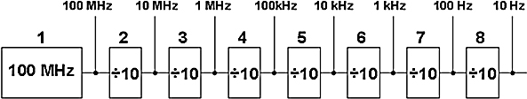
Split Half Method
Many electronic systems do not have only series connected blocks.
They may have feedback loops or parallel branches in a part of the circuit.
Hence use of this method is very restricted.
Divergent Path:
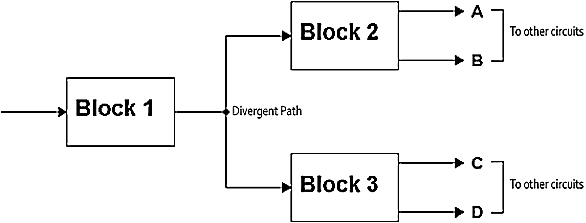
Divergent Path
Here the output from one block is fed to two or more blocks. In such systems, it is best to start by checking the common feed point. Alternatively if the output is normal (at A or B in fig) check the divergence point. Conversely, if one output is abnormal, check before the common point. The most common example is that of the power supply circuit which supplies dc power to various subsystems in equipment.
Convergent Path
In the convergent path two or more input lines feed a circuit block:
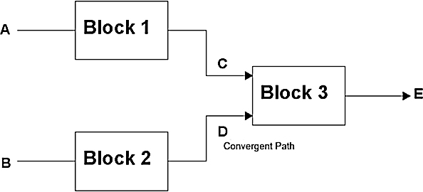
Convergent Path
In order to check such a scheme, all inputs at or before the point of convergence must be checked one by one. If any of the inputs is incorrect (at C or D in fig.), then the fault lies in that particular input circuit. If all are found to be correct, the fault lies beyond the convergent point. For example, if C and D are correct and there is no output at E, the fault lies in unit 3. But if input at C is faulty, the fault lies in block 1 or before that.
Feedback Path
The feedback loop usually corrects the output of the block with the input of an earlier block via a network called feedback network. Since the circuit behaves as a closed loop, any fault within the loop will appear as if the output in all blocks within the system is at fault:
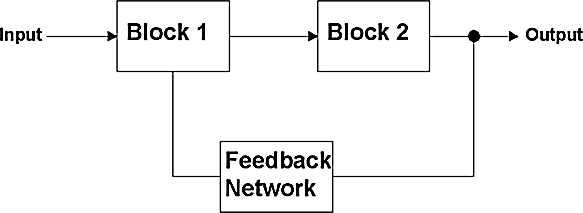
Feedback Path
Before starting troubleshooting of a system having feedback loop, the type of the feedback and its use should be understood well. Feedback paths are provided basically for the following functions:
- To modify circuit function —- Feedback loop is provided to modify the characteristics of the system. For example an automatic gain control system in a radio receiver.
- To sustain circuit function —- Feedback is totally essential for an output to exist. For example an Oscillator circuit.
Having identified the type of feedback circuit, one can proceed as follows to locate the fault.
For the first type, i.e. modifying feedback, it may be possible to break the feedback loop and convert the system to a straight linear data flow. Each block can then be tested separately without the fault signal to be fed around the loop. In some cases instead of completely breaking the loop, the feedback can be modified at or near the point where it rejoins the main forward path. If the output appears normal, check the feedback path, otherwise, check the forward path.
For the second type, i.e. sustaining type, feedback is disconnected from the output and a suitable test signal is injected to check the performance of various circuit blocks.
Switching Path:
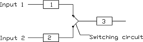
Fault Location in Switching Path
If a system has switch-able parts and if the circuit function is found faulty in one position of the switch, then throw the switch to another position. If the problem persists, check after the switch in common circuitry. If the problem disappears with this action, check that the circuitry is switched out.
- Following are the causes of failure:
Design Deficiency
- Little engineering efforts and changes in design
- Improper choice of components
- Upgrading of a part
- Inadequate information on failure analysis of components
- Insufficient design criteria
- Insufficient prototype testing for meeting both reliability and performance specification
- Excessive heat development inside the equipment and lack of cooling
- Poor mechanical layout of components, assemblies and panels
Production Deficiency
- Imperfection in purchase of material for substandard manufacturer or company
- Unsuitable storage method and unduly long storage period of components
- Absence of training programmers to employ correct and effective production techniques
- Negligence in performing environmental tests like temperature cycling, operation of equipment at elevated temperature for specified period
- Lack of proper working environment, poorly ventilated, poor illumination and dusty assembly shops
- Lack of inspection of goods, sampling tests and inspection
- Insufficient testing and inspection of finished product
Processing Deficiency
- Incomplete or ambiguous specification, specification of unsuitable processing procedures
- Changes in the specification without complete evaluation
- Improper heat treatment, electroplating, welding
- Cold forming, machining, improper identification marking
Assembly Errors
- Undetected errors in assembly by the manufacturer or the purchaser
- Improper matching of various signals used or generated by the components on the terminal board at the time of assembly
- Improper prescribed order of the components collected on the terminal board
Careless Storage and Transport
- Undue long storage of equipment before its dispatch to the customer
- Improper packaging which may be unable to protect the equipment from corrosion or mechanical damage
- Excessive vibrations and mechanical shocks during transportation of equipment from manufacturer to the user
Improper Working Conditions
- Presence of abnormally severe conditions of speed, temperature, loading and lack of dust free areas, air-conditioned rooms
- Using the equipment without following manufacturer’s instructions, warnings and cautions
- Inadequate maintenance policy and after sale service by the manufacturer
- Usage of the equipment beyond its lifetime
- Aging of the equipment
- Poor operating ability of the equipment with the possibility of a high degree of operator error
- Lack of preventive measures
Section 2
- b
- a
- a
- b
- a
- a
- It measures hfe characteristics under DC operating conditions
- a
- b
- The SiO2 layer is so thin, that if a static charge of it is applied across the gate and channel, then the oxide layer may rupture
- c
- b
- Infinite input impedance
Zero output impedance
Infinite open loop voltage gain
Zero offset
Infinite bandwidth - Oscilloscope and Analog Multimeter are the most widely used test and measuring instrument in electronic troubleshooting.
Oscilloscope
Oscilloscope is an instrument which gives a visual indication of what a circuit is doing and shows what is going wrong more quickly than any other instrument. Multimeter can detect the presence of signals and if the shape of the signal is known the average, peak, rms or peak to peak can be calculated. However, if the waveform is not known, then this is not possible. Noise may be superimposed on the signal and the multimeter will not be able to give the proper information. The oscilloscope gives the true and clear picture of the waveforms.
The following figure shows all the essential controls on the front panel. The controls can be present in some different form than shown, but they have to be present in the oscilloscope.
Controls on an oscilloscope
The controls are as follows:
- ON/OFF control
- Focus Control
- X and Y position controls
- trigger, sync or Level control
- Intensity or Brilliance control
Sometimes the ON/OFF control can be combined with Intensity/Brilliance control.
The instrument is directly plugged in to the mains supply. After switching on the instrument, wait for a while until the CRT heater warms up. Turn the Brilliance control in a clockwise direction until you observe a horizontal line on the trace on the screen.
If the trace does not appear on the screen then turn the Brilliance control right up to the fully clockwise direction. Turn Time/cm control to the slowest speed, but not to the off position. With these settings, a light spot should appear on the screen moving slowly from left to right.
Again if nothing is seen, adjust the Trig/Level control in a clockwise direction and observe if something is seen. Adjust the vertical and horizontal position controls until the trace appears.
If all the above steps do not result in showing a trace on the screen, the instrument is faulty. Unplug the mains and check out the fuses.
After getting a trace on the screen use vertical and horizontal position controls to start the trace at the left hand side of the screen and lie along the centre line. Focus control is used to get the line as thin as possible. Reduce the Brilliance setting to a comfortable viewing level.
When making oscilloscope measurements, a pair of probes is very valuable and this facilitates making a contact on the point of measurement in a convenient manner. Probes connect the measurement points in the device under test to the inputs of the oscilloscope. The oscilloscope is used to measure the amplitude, frequency and phase difference as follows:
Measuring Amplitude with Oscilloscope
Oscilloscope greatly and effectively helps in finding out the amplitude of voltage:
Voltage measurement
The number of centimeters on the vertical scale from the negative peak to the positive peak is counted. This count is multiplied by the setting of the volts per centimeter switch.
For example: if 5 V/cm is the volts/cm setting and the waveform measures 4.8V from peak to peak then the waveform voltage is 4.8 * 5 = 24V Peak to Peak.
Measuring Frequency with Oscilloscope
For frequency measurement the time period of one complete cycle is measured. This is nothing more than the horizontal distance between the two identical points on the neighboring waves:
Frequency measurement
This distance is then multiplied by the setting of the Time/cm switch and the period of one cycle is calculated. The reciprocal of this time is nothing more than the frequency of the wave.
For example if the peaks of the waveform are 5 cm apart, and the Time / cm switch is set to 200 μ s / cm, the time of one complete cycle is 5* 200 = 1000 μ s = 1 ms and the frequency is 1 / 1000 = 1 KHz.
Measuring Phase Difference
If we have two signals of the same frequency and wish to measure the phase difference between them, this can be done using a dual trace oscilloscope. One signal is fed to CHANNEL1 input and the other to CHANNEL2 input.
The VH1 position is adjusted to place the CH1 Trace so that it is centered about the horizontal axis of the screen. The CH2 trace is then moved to place it over the CH1 trace. The X position control is then adjusted to move the point where the CH1 trace crosses horizontal axis to line up with the left hand vertical line.
The distance between the crossing point of the CH1 trace and the corresponding point of CH2 trace is then measured along the horizontal axis as shown in the following figure. The total period of one cycle of CH1 waveform is also measured:
Measurement of Phase difference
The phase shift will be the difference in position between the two traces divided by the total wave period and the result is multiplied by 360 to get the phase in degrees.
Analog Multimeter
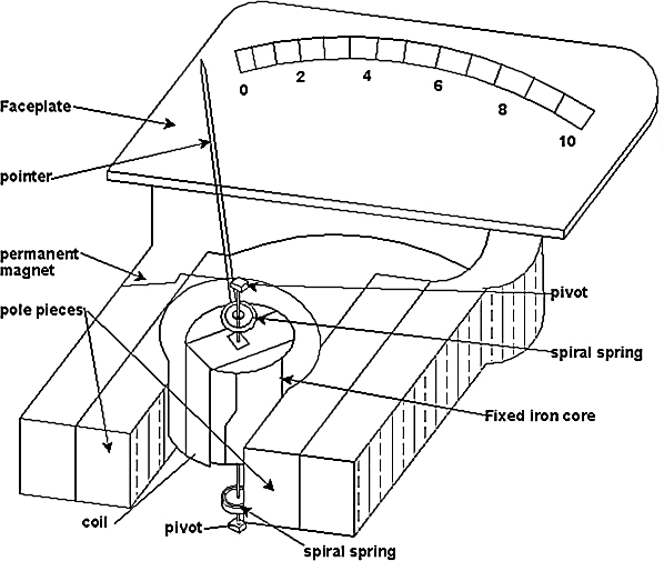
The analog multimeter is the most widely used test and measuring instrument. It operates with a permanent magnet moving coil, which can become a DC voltmeter, an AC voltmeter, and DC milli-ammeter or an ohm meter. Sometimes an AC current measuring facility is also present. It has a coil of fine wire wound on a rectangular aluminum frame. It is mounted in the air space between the poles of a permanent horse-shoe magnet. Refer to the above figure.
When an electric current flows through the coil, a magnetic field is developed that interacts with the magnetic field of the permanent magnet to force the coil to rotate. The direction of rotation depends upon the direction of electron flow in the coil. The magnitude of the pointer deflection is proportional to the current. In usual meters, the full scale deflection (FSD) is about 90 degrees. An analog multi-meter can be used to measure current, voltage and resistance as follows:
Measurement of Current:
The moving coil meter is basically sensitive to current and is therefore an ammeter. For the direct current measurement, place the meter (ammeter to measure current) in series with the circuit. When the ammeter is included in the circuit, its internal resistance adds up, thereby reducing the current in the measuring branch. Usually, this resistance is small and can be ignored.
For alternating current measurement, rectifier type meters are used which will respond to the average value of the rectified alternating current. The meter has to be calibrated in amperes rms (root mean square) for the measurement of sine waves.
Measurement of Voltage:
The current meter can be used to measure voltage. The moving coil meter has a constant resistance. So the current through the meter is proportional to the voltage.
To measure the potential difference between two points, connect the two voltmeter leads to these points. In contrast with the ammeter, the voltmeter is connected in parallel with the circuit whose potential has to be measured.
To measure AC voltage, rectification is required. As in the AC current meters, AC voltmeters respond to the average value of the rectified voltage but are calibrated in volts rms for a sine wave.
Measurement of Resistance:
The moving coil meter can be used to measure unknown resistance. Test probes are short circuited and the ohms adjust control is turned so that the current through the total circuit resistance has a full scale deflection.
An ohm meter is never used while the circuit is in operation. Sometimes the resistances depend upon the circuit conditions, in that case measure the voltage across the resistance, current through it and calculate the resistance.
- Following is the process of testing of MOSFET.
The usual failure mode in a MOSFET is short between the gate and source and the drain and source, i.e. everything is connected together:
MOSFET Test Circuit
A method of testing FET, whether JFETs or MOSFET, involves checking to see if the appropriate voltage on the gate causes the devices to conduct current from source to drain. A simple ohm meter check may not be used with MOSFET, although a check of PN junction from gate to source or drain will give some indication of correct operation in a JFET.
A go/no-go test that is appropriate for N-channel depletion types (JFETs or MOSFET) and P-channel enhancement type (MOSFET) is shown in the above figure.
For an N-channel depletion type, when the switch is open sufficient drain current should flow through the 270 ohm resistor to forward bias the bipolar transistor, and the LED should glow.
If the switch is now closed, the FET should be biased off, and the light should go off. If the LED lights no matter which position the switch is the FET is shorted. If the LED does not light in either position of the switch, the FET is open.
For a P-channel enhancement type, the reverse indications of the LED would be observed. By changing the polarity of the gate supply, other transistor types (P-channel depletion, N-channel MOSFET) may be tested.
Section 3
- c
- c
- c
- Logic clip
Logic probe
Logic pulser
Logic current tracer
Logic comparator - a
- Shorted gate to + VCC
Open gate inside
Shorted gate inside
Open connection to the pin
Short between gate to gate and
Short between gate and ground - a
- c
- c
- Input rectifier and filter
High frequency inverter
Output rectifier and filter
Feedback and control circuit - a
- Faulty transistor
- b
- In a microprocessor based system, if the microprocessor fails to operate as per the requirement, the signals that should be first tested are clock signal, reset signal, address and data lines.
Clock Signal:
The clock signal is tested first, because it is one of the inputs to the microprocessor. If the clock signal is at fault, the whole working of the system may break down. It may stop working or may show intermittent behavior. The clock pulse is tested with a logic probe or oscilloscope. In modern CPUs the clock generator is built within the chip and it only requires an external crystal. The working of the crystal and the capacitor in the clock circuitry is also checked.
Reset Signal:
The reset signal makes the microprocessor go back to a known starting point. When the reset key is pressed, the pin should go low and then return to high. A logic probe can be used to check the presence or absence of a reset signal. At the key, if absence of a signal is noticed, then the reset signal line is checked.
Address and Data lines:
A problem which can occur with address and data lines can be a short circuit with one of the data or address lines on the printed circuit board. The lines can be shortened to the power supply (+5V DC), or it can be shortened to ground. Again a logic probe is used to check these lines. Each line should show activity which should be observed carefully whether it shows a steady high or steady low indicating a short to power or ground respectively. The address and data lines are associated with tri-state buffers. If there is any failure in any one of these buffers, the correct signal will not reach the CPU. If the suspected faulty line does not show a short or break and tri-state buffers are also working fine, then there is a possibility of a problem in the other ICs associated with the line.
- The two schemes that are usually employed for protecting linear regulators are discussed below.
Fold back Current Limiting:
This makes the power supply to switch, give almost zero output voltage if the value of the load current is exceeded beyond its specified range:
Fold back current limiting circuit
An SCR is the device which is used to limit the current.
A current monitoring resistor is placed in the power supply return line.
The voltage developed across this resistor is used to switch on SCR.
In case of an overload, SCR is switched on and the voltage across it falls to approximately 0.9V, which is insufficient to forward bias the series transistor.
The result of this is an appearance of zero voltage across the output.
If SCR is triggered on once, it remains on and until the fault is removed, after switching off the power supply, the output will remain zero.
Over Voltage Protection:
Over voltage protection is required for all the digital circuits. If their Vcc terminal receives more voltage than required, then the ICs get damaged.
A zener diode is used to achieve the over voltage protection:

Over voltage protection circuit
The zener senses the voltage across the power supply’s output terminal.
When the DC voltage rises, the zener starts conducting. This turns on SCR Q2.
The voltage at Q1 collector falls rapidly to zero and the fuse blows.
The above circuit can be called Crowbar Circuit, which limits the output to the pre-set value.
Section 4
- b
- a
- c
- b
- c
- c
- a
- b
- a
- a
- b
- a
- NEXT —- Near End Cross-talk
FEXT —- Far End Cross-talk
PSNEXT —- Power Sum Near End Cross-talk - a
- b
Signal Injection
The system troubleshooting is done by starting at one end and working towards the other, most of the times. However you can save time by starting in the middle of the system. In such a case, you can divide the system in half and reduce the time for troubleshooting.
Usually a signal is injected in the system when you are starting in the middle of the system. There is a simple device called signal injector which injects a pulse or a wave (square) into the system being tested. In case of a pulse, its high harmonic contents make it useful over a wide range of frequencies. Signal Injectors can be used in RF, IF and audio stages because of their broad harmonic content.
In many types of equipment we can inject a test signal of suitable frequency into the input of the equipment and utilize the inbuilt detector or indicator to test its presence at output. Should the applied test signal fail to be indicated in this way and if we are sure that the indicator is OK then we will be pretty sure that the failure is somewhere in the stage or stages between the point of injection of the test signal and the indicator.
Some technicians use the blade of a screw driver for signal injection when they are working away from their work bench instruments. Using a screw driver blade needs a certain amount of skill and experience. For example, if you tap the center tap of the volume control of a speaker with a screw driver, then the volume control is set for high volume after performing this test.
Consider the following figure in which signal injection is used to locate a defective amplifier in a dead system:
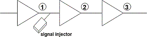
Signal Injection
The idea behind this method of testing is to inject a signal into each amplifier one at a time, and then observe the output of the system. If you start by injecting the signal at 1, then 2, then 3, and so forth, you will not get an output signal until you have gone past the trouble. So, if you inject the signal at 2 and do not get the output, but inject at 3 and do get the output, the trouble must be before 3.
There is an advantage of injecting the signal in the sequence described above. Each time you move the signal source, the output signal will get weaker unless you increase the strength of the signal from the signal generator.
This is better than starting at the output and moving back. Moving the other way requires a relatively strong signal to be injected at the output. When moving back to the previous amplifier, you can overdrive it enough to cause damage.
Signal Tracing
In this technique, a signal is injected at the input and the path of the signal through the system is traced. In signal injection, the signal is injected at each stage and the output is monitored. However in signal tracing the signal is injected at the input itself.
This method speeds up the fault finding process. It includes equipment called Fault Traer which has its own indictor. This may be as simple as a headphone. Usually the oscilloscope is an ideal signal tracer. The idea is to trace the signal between the input and the output at various points, by sampling the signal.
In order to trace the signal a good oscilloscope is used, and with the help of which, you can look at the signal at various points along the signal path. Refer to the following figure:
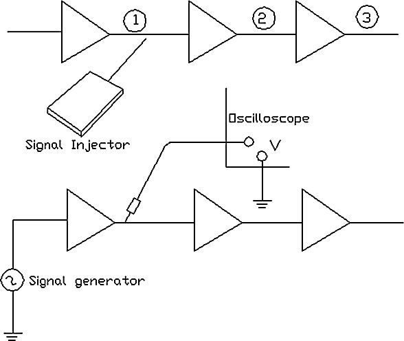
Signal tracing
If the system is audio system, then instead of an oscilloscope, a speaker or a headset can be used to trace the signal.
Resistor Noise
In order to understand the concept of resistor noise, let us take an example of a perfect amplifier. A perfect amplifier is the one which increases the amplitude of an input signal, but it does not add any noise to the signal output.
When there is no input signal and if the wattmeter is connected to the output terminal, then it will show no power output in a perfect (ideal) amplifier. However in a practical amplifier, the wattmeter would show some output power without an input signal. What can be the reason?
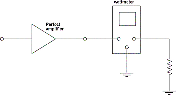
A perfect amplifier
The reason is the noise which is generated within the amplifier. If a resistor is connected across the input of the amplifier, as shown in the following figure, then the output wattmeter shows a measurement, even though, the theoretical amplifier still does not produce any noise. This output measurement is known as Noise Power:

A resistor causes noise in amplifier
The noise power is generated because the amplifier increases the amplitude of the noise generated by the resistor.
In the above circuit no current flows through the resistor R. Obviously then the noise is not created by electrons bumping into atoms and other electrons as they move in a current flow. Then, where does the noise come from? The following discussion helps you out!
Consider the model of a resistor as shown:
A model of a resistor at room temperature
Let us not apply any voltage to this resistor by an outside source of power. The atoms in the resistor are in continuous motion called “Brownian Motion”, at room temperature and at all temperatures above absolute zero.
At room temperature some electrons escape from the atoms for a short period of time. They continuously flow through the material until they are absorbed by another atom that has already lost an electron.
The current caused by this type of motion of the electrons for a very short duration of time is known as intrinsic current.
The electrons move randomly in the material. But at any specific instance of time there will be more electrons moving from one direction to another. At that instant of time a voltage drop is created across the resistor.
When the temperature of the resistor is increased, there will be more electrons moving in the intrinsic current. A voltage is developed across the resistor, whenever the net amount of intrinsic current flowing in one direction is greater than that flowing in the other direction. The higher the temperature, the higher is the amplitude of the voltage. This is because at higher temperature there is more intrinsic current.
The voltages created by the random electron flow in the resistor result in fluctuations over a period of time. Hence for the above amplifier, there is a random fluctuation of voltage at the input.
The random fluctuation is amplified by the (perfect) noiseless amplifier and creates the output noise power. Most amplifiers have resistors at their input terminals and those resistors will produce noise. This noise is very troublesome in some systems. If the noise is greater in amplitude than the incoming signal, then the SNR (signal-to-noise ratio) is very unsatisfactory.
Section 5
- a
- b
- b
- a
- b
- Conventional
Surface mount technology
Surface mount and conventional mix
Double sided laminate
Multi-layer
Flexible PCB - b
- b
- Test pads are the contact points which are specially made for testing. The test probe tips make contact with the test pads.
- a
- Choosing the right equipment
Selecting a supplier
Ordering spares, and
Warranty - c
- Loose connections of electric wires
Smoking
Overloading on electric wires
Short circuiting of electrical wires
Careless storing of inflammable materials
Troubleshooting of Surface Mounted PCBs
Troubleshooting of faulty SMT assemblies usually require removal and replacement of components. The need for troubleshooting arises when there are damaged pads and tracks due to inappropriate or careless component removal practices. These damages are mostly due to inadequate training of the repair workers in properly understanding and handling the SMT PCBs.
The simplest method to remove the faulty components is cutting all leads. Each leg is cut carefully and then the component is taken off. Each joint is then melted with a fine tip, temperature controlled soldering iron and remaining IC legs are removed with tweezers. The tweezer uses the squeezing action to remove a variety of parts. After allowing a cool down period, excess solder is removed with a de-soldering braid. This method does not require any tool and special workstation; hence it is cheap. But it can damage the components while cutting, thus in turn damaging the PCB substrate and copper pads. Also, soldering the replacement component in position using a soldering iron requires processing one lead at a time. Hence it is time consuming also.
In order to rework the SMT PCBs, two basic heating methods are introduced. These methods are conductive and convective methods. Let us understand these methods:
Conductive Method
This method uses a heated tool that contacts the solder joint to effect reflow. The soldering tools are provided with the tips designed to heat all the component’s leads. Their electrodes come in contact with component legs and hold them flat to the copper pads on the PCB.
Sometimes a controlled pulse of current is also used which passes through the electrode which heats the component leads. This melts the solder on the joints and the built-in vacuum pick-up lifts up the component from the surface.
The technique enables all the leads to cool down rapidly after the soldering operation and so allows the leads to be held in position while the solder solidifies. The conductive does not heat the component body and it is very fast and repeatable.
It is very good for replacement as the electrodes will hold the legs flat to the pads during the solder reflow, while the alignment and positioning is ensured with microscope. The process is a little expensive.
Convective Method
It is known as hot gas soldering where hot gas or hot air is used as the heat transfer medium. The hot gas is swept over the leads until full reflow is achieved, after which a part is lifted with a tweezer.
Small parts such as chips, transistors, SIOC and flat packs can be removed with a single point nozzle. With longer components, a component specific nozzle is fitted to the hand piece and brought around the part to remove the surface mounted devices.
The vacuum pick-up lifts up the component after reflow. Sometimes infra-red radiation is also used for re-flow of the solder joints. The process takes a longer time for removal as compared to conductive method.
Removal of SMDs
The following steps should be performed for removal of a component using a hot gas machine:
- Apply a small amount of liquid flux to the joint.
- Chose the correct head to suit the component.
- Keep the PCB in place and activate the gas flow to reflow the solder on every joint. A Video Display Unit or microscope can be used.
- If the component has been bonded with an adhesive, rotate the head to shear the bond.
- Remove the component with the vacuum pick-up and allow the PCB to cool.
- Remove any remaining solder with the help of de-soldering braid.
- Allow a further cool down period and lastly inspect the pads to ensure that they are not damaged.
Replacement of SMD
The following procedure is followed for replacement of a component:
- The new component is inspected to ensure that the legs are not bent or distorted.
- A thin film of flux is lightly applied to the pads.
- The component is then placed into the head of the hot gas machine and carefully lined up to the PCB.
- The components are lifted away from the board until the legs are just clear of the pads. Then the gas flow is initiated. The applied gas heats up the legs and the solder on the pads.
- At the time when the solder is flowing, the legs of the components are made to sit between the fingers of the tape and hence are central over the pads.
- Make sure that the solder flows correctly around each leg, until then the gas is allowed to flow.
- Stop the flow of the gas when the solder is distributed evenly around the leg and allow the board to cool at least for one minute to avoid disturbing the joints.
- Remove the PCB from the machine and then carefully remove the Solder Quick tape and clean all the excess flux from the joints.
- Inspect all joints with magnifier to ensure correct reflow.
- Clean the PCB with isopropyl alcohol in aerosol form to ensure penetration of the solvent under the component to wash out any flux. The area can then be brushed to remove all traces of flux.
Preventive Maintenance:
Preventive maintenance means all actions intended to keep equipment in good operating condition and to avoid failure. A good preventive maintenance program is the heart of effective maintenance. It is an activity designed to prevent wear and tear or sudden failure of equipment. It involves a policy of replacement of components of a system before the component actually fails. Let us see the Advantages of Preventive Maintenance Preventive maintenance implies frequent inspection to detect minor faults and the early correction of them, supplemented by periodic overhauling in accordance with a plan so that a possibility of major breakdown is almost entirely eliminated.
An equipment in good working order subjected to regular inspection and adjustments will continue to produce quality products for a longer period than otherwise. An efficiently managed preventive maintenance system improves working conditions and therefore it has a great importance amongst all types of maintenance. For continued, good service of equipment, the equipment has to be in a good working condition. If this is accepted, it becomes obvious that the preventive maintenance system guarantees the continued good working of equipment.
In fact, preventive maintenance occupies the same position with regard to equipment as preventive medicine does with regard to public health. If preventive maintenance is performed at predetermined periods and coordinated with the production schedules, the quantum of production will automatically increase. A branch of preventive maintenance called “Predictive Maintenance” applies sensors and analysis of technical data to determine when the performance of a piece of equipment is about to degrade or when it is about to break down. It is intended to prevent breakdown. Predictive Maintenance is a program of periodically monitoring equipment and tracking certain measures of its performance. Predictive Maintenance is more feasible today because of the technology that is available for equipment surveillance and diagnosis of problems while the machines are still running. The condition of equipment can be monitored by several means. Critical monitor points on the equipment are identified. Sensors may be installed or periodic readings may be taken with portable units to measure the temperature or vibrations. Vibration sensors and ultrasonic sensors are used to feed data into a computer for analysis.
A program of this type prevents unplanned downtime that disrupts production schedules, creates an idle work force and degrades customer service. Equipment is out of service for a very short duration because much of the diagnostic work has already been done and the necessary parts and people are available.
Section 1 (Covers chapters 1 and 2)
Single Line or Multiple Choice Questions
- Which one of the following is easier to replace?
- A battery
- A transistor
- Should the troubleshooting technician totally depend on the symptoms?
- YES
- NO
- If a system is suspected to be faulty, which one of the following would you test first?
- Transistor
- Power supply
- Signal generator, if present
- If an equipment starts malfunctioning when it warms up, then usually the reason for this can be:
- Malfunctioning of power supply
- Dryness of electrolytic capacitors
- Melting of the leads of components
- Use of split half method is restricted because:
- Many electronic systems do not involve only series connected blocks
- Many electronic systems can not work under high frequency conditions
- Many electronic systems can not work under low frequency conditions
- In electronic equipment, what is the purpose of an edge connector?
- Connects the edges of the PC board to the card rack
- Brings signals and power to and from the circuit board without using a wire to the circuit board
- Define reliability.
- What are the three stages in the failure curve?
- What is a catastrophic failure?
- A sudden and complete change in the performance of equipment
- A gradual and partial change in the performance of the equipment
- A complete breakdown of the equipment
- Define Mean Time To Repair.
- If you take reciprocal of constant failure rate, then it becomes:
- MTTF
- MTBF
- MTTR
Descriptive Questions
- Explain the process of troubleshooting from the point of view of Fault establishment, Fault Location and fault correction.
- Write a short note on symptoms.
Section 2 (Covers chapters 3 and 4)
Single Line or Multiple Choice Questions
- Allen wrenches are also known as:
- Circular Socket Bar Spanner
- Hexagonal Socket Bar Spanner
- Which tool is used to acquire electronic fabrication?
- Files
- Screw drivers
- Wrenches
- How is the voltmeter connected when the potential difference between two points is being measured?
- In series with the circuit whose potential has to be measured
- In parallel with the circuit whose potential has to be measured
- The polarity of the leads of the analog multi-meter is not important when measuring AC quantity. Choose the correct answer:
- TRUE
- FALSE
- They have high input impedance and the user has to only set the function switch and read the measurement. Which instrument does this information relate to?
- Analog multi-meter
- Digital multi-meter
- Which instrument will you use in order to measure phase difference between two signals?
- Waveform Generator
- Oscilloscope
- A Tunnel diode is not checked with an Ohm-meter. The statement is:
- TRUE
- FALSE
- Can you use an ohm-meter to determine if the diode will operate properly at its specified zener voltage?
- Yes
- No
- The most important advantage of FET over BJT is:
- It gives extremely high input resistance
- It gives extremely low input resistance
- How is a MOSFET protected from static charges when not in use?
- Leads are covered in plastic material
- It is wrapped in a piece of cloth
- Leads are shorted together and are placed into conducting foam material
- An ideal op-amp should have:
- Infinite voltage gain
- Zero voltage gain
- A circuit which can produce accurate highly stable time delays is:
- Op-amp circuit
- Timer IC555
- If diodes, transistors and in-circuit semiconductors are to be tested with an oscilloscope, then:
- Oscilloscope should be set in component test mode
- Oscilloscope should be set in TV trigger mode
Descriptive Questions
- Explain testing of a semiconductor diode and a tunnel diode.
- What are the common problems associated with RS-232? Explain how the switches are tested?
Section 3 (Covers chapters 5 and 6)
Single Line or Multiple Choice Questions
- Give one example of an Analog and Digital System.
- To which logic family does 74LS belong?
- CMOS
- ECL
- Low Power Schottky TTL
- What is the reason for output Stuck at ‘0’ for a gate?
- 0V line is open circuited internally
- VCC line is open circuited internally
- There can be an open lead which can be either an input or an output pin
- In digital systems, which troubleshooting equipment is used to stimulate digital circuits:
- Logic Probe
- Logic Pulser
- Logic Current Tracer
- For testing of IC, if a series of pulses is given to step the IC into various steps and then the steps are monitored with the help of an oscilloscope. Which test is this?
- AC Test
- DC Test
- Functional Test
- The process of Rectification makes the output voltage independent of line and voltage variations. The statement is:
- TRUE
- FALSE
- A ‘trimmer pot’ is used to:
- control high or low output voltage in a power supply
- control high or low output current in a power supply
- In order to protect linear voltage regulators by a fold-back current limiting system which of the following devices is used?
- Transistor
- SCR
- Diode
- Electrically which device creates more noise?
- Series type regulator
- SMPS
- Name any four types of oscillator.
- Ground loop means:
- Loops are created around various ground points
- Difference in current between various ground points
- Difference in potential between various ground points
- For which class of amplifiers does the Short Circuit Voltmeter Test not work?
- Class A
- Class B
Descriptive Questions
- Write a short note on Logic Pulser and Logic Current Tracer.
- Explain the block diagram and testing of SMPS.
Section 4 (Covers chapters 7 and 8)
Single Line or Multiple Choice Questions
- What is the effect of temperature on failure rate?
- Failure rate becomes half with every 10 degree rise in temperature
- Failure rate doubles with every 10 degree rise in temperature
- Failure rate becomes 3 times with every 10 degree rise in temperature
- A positive temperature coefficient means:
- Resistance increases with rise in temperature
- Resistance increases with decrease in temperature
- A Sensistor is a device with:
- Positive temperature coefficient
- Negative temperature coefficient
- Zero temperature coefficient
- How does a Thermal Fuse protect the circuit?
- It absorbs the excess of heat due to a rise in temperature
- It breaks the circuit at specific temperature
- Why is it a good idea to troubleshoot a system by starting in the middle of the system?
- To save time
- Because that is usually the location where the trouble is
- The advantage of using a signal injector over using a screw driver is:
- It provides a quicker method
- It injects a wide range of signals for testing a variety of signals
- Which of the following waveform would you prefer for signal injection?
- Sine Wave
- Pulse
- After preliminary checks, a quick troubleshooting starts:
- At the signal input end of the system
- At the signal output end of the system
- In the middle of the system
- In order to have a satisfactory SNR:
- Noise should be greater in amplitude than incoming signal
- Noise should be less in amplitude than incoming signal
- Noise should be equal in amplitude than incoming signal
- Partition noise is not a problem in:
- Vacuum tube
- Bipolar transistor
- MOSFET
- Flicker noise is present in all amplifying devices. It is an example of:
- White noise
- Pink noise
- List any four types of EMI.
- In order to filter a signal and to isolate the power source using decoupling, the best component is:
- A resistor
- A diode
- A capacitor.
- A material which is used for sealing seams and joints on shield to prevent EMI energy from passing through it is:
- EMI gasket
- EMI shield
- EMI seal
- The most effective filter design for EMI applications is:
- Band pass filter
- High pass filter
- T-filter
Descriptive Questions
- Explain how Thermister and Sensistor compensate against temperature variations.
- Explain Shielding, Filtering and Bypassing in context with electromagnetic interference.
Section 5 (Covers chapters 9 and 10)
Single Line or Multiple Choice Questions
- If a solder goes directly from solid state to liquid state, it is said to be:
- Eutectic
- Electric
- Which of the following materials’s smoke should not be inhaled, as it is poisonous during soldering?
- Indium
- Cadmium
- Lead
- After soldering a wire to a terminal, you should be able to see the outline of the wire and the strands of the wire. Choose the correct answer:
- The statement is TRUE
- The statement is FALSE
- What should be done in order to avoid a cold solder joint?
- It is kept undisturbed and allowed to air dry completely
- A blower is used to cool it
- What is done in the layout stage during the preparation of the PCB?
- A sketch of component location and interconnections of the components is worked out
- Only a sketch of component location is worked out
- Only the interconnections of the components are worked out
- Which solder type should be avoided for Surface mount technology?
- 63/37
- 60/40
- Conductive method and Convective method are the two methods used for troubleshooting of:
- Surface mounted PCB
- Conventional PCB
- What are the two types of Automatic Test Equipment?
- Define maintenance.
- What are three major types of maintenance?
- Corrective maintenance is also known as:
- Breakdown maintenance
- Predictive maintenance
- What are the various groups in a maintenance organization?
- List some first aid materials.
Descriptive Questions
- Write a short note on soldering.
- Explain what is maintenance policy?
Answers
Section 1
- a
- b
- b
- b
- a
- b
- The frequency at which the failure occurs is termed as reliability of the system. The less is the occurrence of failure, the more is the reliability of the system.
- Infant Mortality period
Steady state failure rate period
Ageing period - a
- MTTR is defined as the average time required to bring a system from a failed state to an operational state.
- b
Troubleshooting Process
The process of troubleshooting comprises the following steps:
- Fault Establishment
- Fault Location
- Fault Correction
Let’s see these steps in brief
Fault Establishment
It is important to establish the presence of a fault in equipment before taking any other action. In some cases a system may be reported faulty, but it may be a case of faulty operation or a system failure may be reported with either very little or misleading information. It is essential that a functional test, checking the system’s actual performance against its specification must be made and all fault systems must be noted.
It is also important to check the history of the equipment and repair and servicing work carried out earlier by any other person.
Fault Location
This involves pin-pointing the cause of the fault by studying the literature relevant to servicing, maintenance and repairs. The fault is located first in the subsystem and then in a single component in the subsystem.
Fault Correction
Fault correction consists in replacing or repairing the faulty component. This is followed by a thorough functional check on the whole system:

Troubleshooting Procedure
Symptoms
Symptoms are useful to locate the general area of a problem. The symptoms are sometimes described by the equipment owner or user. In an industrial electronic plant, it may be the foreman of the division who uses the equipment. In consumer electronic equipment, the description is often from the customer who owns the equipment.
The most reliable symptom analysis is given by the technician after energizing the equipment. Technicians know that certain symptoms in a system usually mean that a certain component has failed.
Symptoms are indeed a valuable guide for troubleshooting. However, one should avoid basing a complete troubleshooting procedure on the knowledge of symptoms alone. For example, distortion in a radio’s output sound can be caused by different reasons such as low terminal voltage of aging battery, overuse of transistor, a tear on a speaker cone.
An item is considered to have failed because of one of the following three conditions:
- When it becomes completely inoperable
- When it is still operable but is no longer able to perform its intended function satisfactorily, or
When serious deterioration has made it unreliable for its continuous use, thus necessitating its immediate removal from service for repair or replacement
Section 2
- b
- a
- b
- a
- b
- b
- a
- b
- a
- c
- a
- b
- a
Testing of a Diode
A diode can be conveniently checked with an OHM METER by measuring its forward and reverse resistance. A signal diode shows a low resistance (a few hundred ohms) in the forward direction and a high resistance (nearly infinity) in the reverse direction:

Testing of diode with an ohm meter
a) Forward biased b) Reverse biased
Procedure:
- Connect positive (red) lead to anode of the diode and negative (black) lead to cathode. The ohmmeter shows a low resistance, as the diode is in forward bias.
- To confirm the polarity of the voltage in resistance range, the leads can be connected to a voltmeter to check the correct polarity.
- Reverse the leads, so that the ohm meter shows a very high reverse resistance.
- A short diode shows a low-resistance reading in both the directions and an open diode shows high resistance (infinity) in both the directions.
- On a DMM, select the selector switch to a diode check mode. Using this, a forward biased diode should read between 0.5V to 0.8V and a reverse biased diode should read approximately 1.545V, for a good diode.
Testing of Tunnel Diode
A tunnel diode (TD) is a p-n junction which exhibits a negative resistance interval. Negative resistance values range from 1 to 200 ohms for various types of tunnel diodes. They are utilized in switching circuits. A TD is evaluated using a saw tooth output waveform from an oscilloscope as a current source.
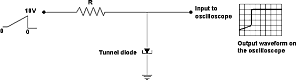
Testing of Tunnel diode
A 670ohm resistor from the saw tooth out connector in series with TD to ground will give a calibrated current/div horizontally (say 1 mA/div).
The saw tooth voltage goes from 0 to 10 volts. Therefore, the horizontal display becomes current/div. Looking at the voltage drop across the diode will give a vertical display of the low / high voltage state of the diode.
The display does not give an indication of switching time but confirms that the device has the ability to switch at the correct current level and will probably perform normally in the circuit.
Common Problems with RS-232C
- No information is transferred
- Unable to communicate with the machine it is connected to
- Any garbled information is transferred
- Only sends or receives files and unable to perform both
- Only a part of a file is transmitted
- Interruption in transmission
Troubleshooting of Switches
Usually a defective switch is not repairable. It is recommended to replace the broken or defective switch. The defects in a switch can be loss of continuity between the contacts, improper spring loading function because of a defective spring, loose toggle, broken or burnt switch body, etc.
In order to make an in-circuit test on a switch a VOM can be employed. The following figure shows how to use a VOM for this purpose:
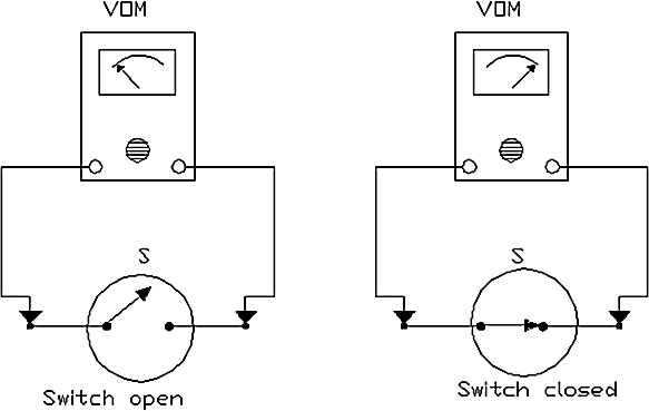
Testing a switch
The meter prods are connected or touched to both the sides of the switch. The meter shows infinite resistance when the switch is in OFF position. When the switch is closed, i.e. ON, the meter shows zero resistance indicating that the two sides of the switch are electrically connected.
If the switches are found faulty, replace the switch. Carefully switch off the power while replacing it. If there are any connections made to the switches, label all the wires connected to it before removing. When the new switch is replaced, connect all the wires in their proper positions. Turn on the power and check the working of the switch by the procedure described above.
Section 3
- Telephone voice signal is analog signal Digital calculator’s output is in digital form
- c
- b
- b
- c
- b
- a
- b
- b
- Colpitt’s oscillator
Hartley oscillator
Wein bridge oscillator
Crystal oscillator - c
- b
Logic Pulser
A Logic Pulser is used to stimulate digital circuits and supplemented by a logic probe it aids in testing for circuit response to easily check gates, lines, buses and nodes. It does the same job in digital systems as a signal generator does in analog systems. It injects a desired signal for the purpose of testing.
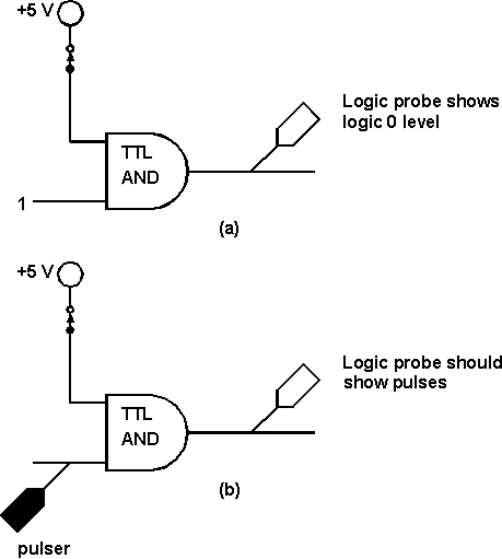
Logic Pulser determines gate operation
The above figure shows a troubleshooting problem where a combination pulser and probe can save time by preventing a wrong interpretation of a measurement.
In figure (a), the logic probe shows a logic 0 output of the AND gate which should be logic 1.
Figure (b) shows how to test for this problem. The pulser injects the signal and the logic probe is used to look for that signal.
If the problem is with the gate, the probe will show a pulse signal. If the point is grounded, the probe will indicate no signal.
Pulse height or amplitude is derived from the power supply that the pulser is connected to. For this reason the pulser should always be powered from the circuit under test or power supply from the same voltage.
The power supply requirements of the pulser are 3 to 18 V dc for CMOS and 4.5 to 5.5 V dc for TTL.
Logic Current Tracer
Current tracing is very effective troubleshooting. It is difficult to isolate a bad element when a given circuit node is stuck in one logic state and several elements are common to that node.
The hand held current tracer has one lamp indicator that glows when it is held over a pulsing current path.
The instrument detects whether current is flowing or not and where the current is flowing. For instance if the node is stuck on LOW state due to a shorted input in one of the devices connected to the node, a very strong current exists between the circuit driving the node and the faulty component.
The use of a current tracer helps to pinpoint the faulty point on a node, even on multi layer boards.
The current tracer senses the magnetic field generated by fast rise time current pulses in the circuit (or, provided by a logic pulser), and display steps, single pulses, and pulse trains using a simple one light indicator:
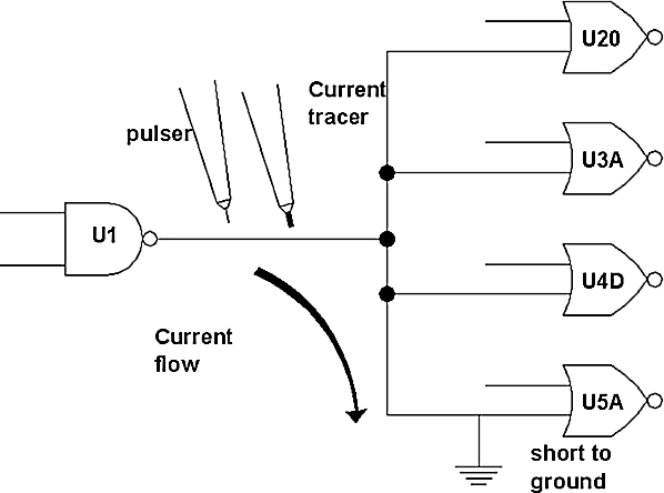
Multiple input fault detection using current tracer and logic pulser
The above figure shows location of a multiple input fault. A logic pulser is used to provide current pulses. Gate U5A is shorted to ground causing the node to be stuck LOW and sinking virtually all current from U1 and other inputs. A current tracer quickly verifies this fault by a clear single lamp indicator on the node.
A current pulser is also used for the following conditions:
A solder bridge fault can be detected using a current tracer.

Solder bridge fault
In the above figure a solder bridge between U1 and U2 causes both nodes to indicate functional logic failures. Tracing current flow in the circuit quickly shows the location and cause of the fault.
It is also known as switching power supply or sometimes chopper controlled power supply. By using a switch as a series element and controlling the on and off time we can vary the average voltage at the DC output level:
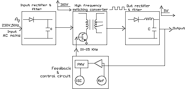
Functional Block diagram
The above figure shows four major blocks of SMPS:
- input rectifier and filter
- high frequency inverter
- output rectifier and filter
- feedback and control circuit
The AC mains are rectified and filtered. The high voltage DC is then fed to the high frequency inverter. The operating frequency range is from 20 KHz to 1 MHz.
The high frequency square wave thus generated is stepped down by the high frequency transformer and then rectified and filtered to produce the required DC output.
The output is compared with a reference and pulse width modulated to get the desired regulation by the control circuit. The regulation of the output voltage is achieved by varying the duty cycle of the square wave.
When the load is removed or input increases, the slight rise in the output voltage will signal the control circuit to deliver shorter pulses to the inverter. Conversely, as the load is increased or input is decreased, wider pulses are fed to the inverter.
The efficiency of an SMPS is higher than a series type regulator. They are physically smaller and lighter than linear regulators.
They are noisy electrically and sometimes audibly. Thus they are unsuitable for powering circuits that are sensitive to electrical noise unless adequate filtering and shielding is provided.
Testing SMPS
When testing SMPS, each branch of the supply will shut itself off, if its load is disconnected. For this reason, a load resistor must be connected to each branch during testing.
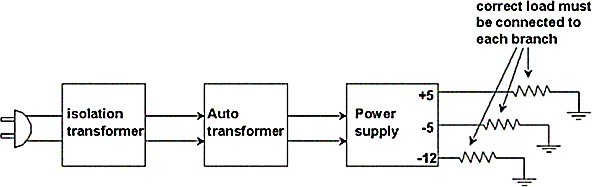
Testing SMPS
The value of the load resistor to be connected would depend upon the current rating of the supply. An isolation transformer and an auto transformer are connected in the AC line during the test. The auto transformer is useful for varying the AC voltage and the isolation transformer is useful for protection.
If this equipment is not available, the troubleshooting of SMPS should be limited to visual inspection for burnt or damaged parts.
Section 4
- b
- a
- a
- b
- a
- b
- b
- c
- b
- c
- a
- System radiated EMI
External radiated EMI
Internal radiated EMI
Conducted EMI - c
- a
- c
Thermister compensation against temperature effects
A Thermister is a device with a negative temperature coefficient, i.e., its resistance decreases with the rise in temperature. The following figure shows a circuit with Thermister compensation:

Thermister compensation
As the temperature increases, value of resistance Rt decreases, and the current in the Thermister increases. This leads to an increase in the current in resistance Re. This increase in current results in an increase in voltage Ve across Re, which increases I2, which in turn reduces the base current Ib. The reduction in base current Ib reduces collector current Ic, thereby compensating for any increase in collector current due to a rise in temperature.
Alternatively, the Thermister can be placed across R2 as shown in the following figure:

Alternate Thermister compensation circuit
When temperature increases, resistance of the Thermister decreases, and the value of parallel combination of R1 and R2 also decreases. This leads to an increase in I2 and a decrease in Ib. This results in a decrease in Ic to compensate for any increase in Ic due to a rise in temperature.
Sensistor compensation against temperature effects
A Sensistor is a device with a positive temperature coefficient, for example its resistance increases with temperature. The following figure shows a circuit with Sensistor compensation:

Circuit with Sensistor compensation
As temperature increases, value of RC increases and hence value of parallel combination of R1 and RC increases leading to a decrease in I1. Thus Ib decreases resulting in a decrease in IC to compensate for any increase in IC due to a rise in temperature.
Alternatively, the Sensistor can be placed either parallel to Re or in place of Re as shown in the following figure:
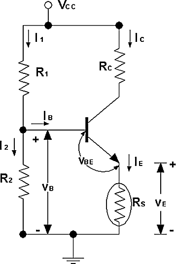
Alternate Sensistor compensation
Any increase in temperature results in an increase in Rs resulting in a higher voltage drop Ve. This increases the voltage at the base, leading to an increase in I2 which reduces Ib. A decrease in Ib results in a decrease in Ic, compensating for any increase in Ic due to temperature.
Shielding, Filtering, Bypassing
Shielding is a process aimed at confining radiated energy to the bounds of a specific region or to prevent radiated energy from entering a specific region. It has been found that the shielding of source is required more as compared to the shielding of receptor, because source is the one which is allowed to radiate (for example, Broadcasting stations).
Shielding is accomplished by two mechanisms: Absorption loss and reflection loss. At low frequencies, shielding is accomplished primarily by absorption loss and at high frequencies it is accomplished by reflection loss. However, the total shielding function is a composite of both reflection loss and absorption loss.
The thickness of the shield can be calculated by simplifying these two phenomena. There is a unit of measurement for shielding called ‘one skin depth’. This is the thickness of the piece of metal which is bombarded with EMI.
A total closed shield isolated from outer world is never possible. The source has to have connections from the outside systems which are power system and load terminals. The shielding can be in a form of partition boxes or cable and connector.
A shield reduces EMI field strength. Shielding is measured and specified in terms of reduction in field strength caused by the shield. A material which is used for sealing seams and joints on shield to prevent EMI energy from passing through it is called EMI gasket.
For example, the following figure depicts a PC board without filtering or shielding:

PC board without filtering or shielding
The electromagnetic energy enters the device along cables and traces by radiation through the air. When filter capacitors are installed, conducted interference is reduced. These filters conduct the desired current but reject the undesirable currents. However, energy can still enter the source by direct radiation.
A shield prevents the radiated EM energy from interfering with the equipment. Thus both filtering and shielding are both necessary to prevent possible EMI problems. With the same purpose as with shielding, filtering is used to solve EMI problems when the circuit is the source of noise. The following figure shows the effect of shielding and filtering:
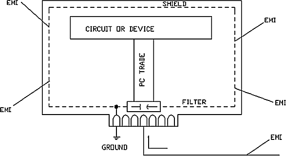
Effect of filtering and shielding
The discrete capacitors and bypass capacitors should be placed as close to the voltage source as possible and adjacent to the active devices if present. In digital circuits, capacitors filtering low frequency supply voltage noise are generally placed adjacent to the voltage input pins. The value of such capacitors can be 10µF or above.
Capacitors filtering high frequency noise should be placed at the IC being filtered. These capacitors are low value capacitors of the range 1µF and below. The ideal position of the capacitor and the IC would be across the supply voltage and ground pins.
EMI filters can be used as a shunt element to divert electrical currents from a trace or conductor; as a series element to block a trace or conductor current; or they may be used as a combination of these functions. Selection of the filter elements should always be based on the desired frequency range and component characteristics.
To filter a signal and to isolate power source using decoupling, a capacitor is the best signal filter within its high frequency performance characteristics. The bypass capacitor greatly reduces the power and ground circuit noise, if they are located properly in design layout.
EMI problems at high frequencies can be reduced by using a low pass filter. It incorporates a capacitive shunt and series resistance or inductance. However, at high frequency, the capacitor can become inductive and the inductor can become capacitive causing the filter to act more like a band-stop filter.
The basic criteria to design a filter should be based on the overall impedance at the circuit’s point of application for proper match. For most EMI applications, a T-filter design is effective and is ideal for analog and digital I/O ports.
Section 5
- a
- b
- a
- a
- a
- b
- a
- ATE with fixed base plate
ATE with movable base plate - Maintenance in an organization is the upkeep, repair, renewal and replacement of worn, damaged, or obsolete parts of equipment.
- Corrective Maintenance
Improvement Maintenance
Preventive Maintenance - a
- Engineering Group,
Equipment Repair and Maintenance Group,
Central Services Group,
Construction or Civil Engineering group, and
General Maintenance Group. - Tincher iodine, Detol, Burnol, Plasters, Bandages, Cotton,
Knife, Scissors, Measuring glass, Antiseptic cream
Eye washing glass, Dropper, Safety Pin,
Stretcher, and necessary capsules and tablets, etc. are required.
Soldering involves removal and replacement of the electronic components from the printed circuit boards. If a component is soldered, it means that there is a continuity of metal. Soldering is an alloying process between two metals.
It is a popular method of connecting circuits. When it is done properly, soldering is a highly reliable and low cost process. Most of the solders used today are 60/40 type, i.e. 60 percent tin and 40 percent lead. A better is of 63/37 variety which has 63 percent tin and 37 percent lead. This alloy is available in wire form and in several gauges.
Most combinations of tin and lead become plastic before they actually melt. So, they have three states: solid, plastic (mushy) and liquid. 60/40 is the plastic state, but there is a very small difference between the liquid and solid state.
The 63/37 solder is eutectic at a temperature of 370°. This means that it goes directly from the solid to the liquid state without having a plastic intermediate step. This is one of the reasons that 63/37 is often used for replacing parts on newer systems where components are very small and sensitive to heat.
The following figure shows the difference between 60/40 and 63/37 when heated:
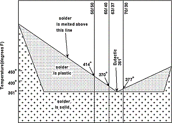
Solder and their melting temperatures
Plastic solders are also available. Instead of soldering with a combination of lead and tin, plastic solders can be used which are soft in state and are hardened by heat or by adding a chemical called a catalyst or hardener. In either case, the plastic solder is applied first and then hardened.
The plastic solders which use catalyst for hardening are useful in surface mount configuration, where heat must be used sparingly to protect the component. Plastic solders form a solid, strong bond and they are easy to apply.
There is one more type of solder called silver solder which employs indium. Another type of solder combines indium, tin, lead, cadmium and gallium. These solders melt at very low temperatures, but they do not flow easily like the more conventional solders. Some solders melt at such low temperatures that they can be melted with the flame from a match.
In its molten state, solder dissolves some of the metal with which it comes into contact. The metals to be soldered are more often than not covered with a thin film of oxide that the solder can not dissolve. A flux is used to remove this oxide film from the area to be soldered.
Process of Soldering
The process of repair of any electronic circuit involves the following major steps:
- Dis-assembly of particular component
- Testing of the component
- Replacement of the component found defective and
- Testing the circuit for performance check
A good soldering practice is required for the removal and replacement of electronic components. The soldering process involves:
- Melting of the flux which, in turn, removes the oxide film on the metal to be soldered
- Melting of the solder which makes the lighter flux and brings the impurities suspended in it to the surface
- The solder partially dissolving some of the metal in the connection and
- Cooling and fusing with the metal
The soldering process needs an understanding of:
- Soldering tools
- Soldering material
- Soldering procedure
- Replacing components
- Special consideration when using MOS and micro-electronic circuits
- Good and bad soldering joints and
- De-soldering techniques
The process of soldering ensures the following steps:
- The soldering iron must be placed at an angle of 45 O to the soldering area
- The solder is placed near the iron and it is flowed. It is passed around the joint until you come back near the iron
- Now, let the solder flow into the area from where the iron has been removed
- All the elements of the joint must be covered with the solder. The joint formed by the solder must be firm.
- The solder is taken away, when it is ensured that the solder has flowed into the leads and tracks. First the solder is removed and then the iron is taken away. If the iron is removed first, it will result in a dry joint, due to the solder taking heat from the joint prematurely.
Maintenance Policy
In any organization, whenever new equipment is purchased or a replacement of an existing worn out equipment is planned, the maintenance department has an important role to play. However, right selection of equipment holds the key to form a good maintenance policy. The maintenance policy must consider the following important points for successful maintenance:
- Choosing the right equipment
- Selecting a supplier
- Ordering spares and
- Warranty
Let us see all these points one by one.
Choosing the right equipment:
- The user must be sure that he is buying equipment that he really needs. He should be able to select the equipment which will best suit the economic as well as technical range.
- The technology changes everyday. So, keep track of changing technologies. Some technologies are progressing so rapidly that it has made the job of selection difficult.
- For choosing the right equipment, always look for performance and features. There are many new types of equipment that have user friendly features that make measurement and operations easier. But this should not affect the overall performance. The difference between performance and features must be clearly understood.
- The person, who is selecting the equipment, should have prior knowledge about the exact requirement and the current equipment available in the market which fulfills the requirement. Usually, the concerned maintenance engineer does this job. The engineer should contact the maintenance department before placing any order.
- The purchase order should be placed properly. The person, who is ordering the purchase, should go through the purchase contract thoroughly. The purchase order should insist on complete documentation, warranty period, free service period, training in operation as well as in maintenance, installation, discount if given.
Selecting a supplier:
- Ensure that the supplier has the proper infrastructure to make the product. The purchase function has what is known as the Vendor rating in which the capacity of the supplier to manufacture as per certain standards is asserted and is given a rating. This will ensure reliability in the supply.
- A branded supplier will guarantee a basic quality standard and very little inspection is required. On the other hand, a smaller supplier may supply the equipment as per the purchase order, but may have problems in long term reliability. We must assess a supplier before we place an order on him.
- For special purpose machines we must remember that making a proposal is a time consuming and costly affair. Do not ask for proposals from too many suppliers as it requires a lot of time to evaluate the proposals.
- The purchase order for a special purpose machine should be the culmination of countless discussions with a comprehensive statement of the work to be done, engineering and machine acceptance terms, payment terms, installation, documentation, training, etc.
- If the system can be divided into many parts or functions, then it is better to break up the cost of each function so that in case of subsequent modification, the implications on the cost can be worked out.
- For imported equipment, the major issue can be the distance between the user and the manufacturer. Spares have to be stocked in larger quantity. Make sure that the document and the manuals are in the English language or in local language.
Ordering Spares:
- The components in electronic equipment are manufactured by several specialized companies. The equipment manufacturer gets the components from these suppliers of components. Sometimes the components are purchased from a trading agency.
- While ordering spares, the person in charge, should have a sound knowledge of the component number, name of the component and its description, name of the company, etc.
- The manufacturers have their specialized way of coding for the component number which is denoted by the component number. The component number specifies the assembly reference and the component circuit reference.
- Many components are selectable, i.e. the equipment manufacturer selects the components from a batch supplied by the component manufacturer that meets the manufacturer’s specifications.
- In case of imported equipment, spares may not be available in the local market and will have to be imported. This takes considerable time and money. So it advisable that a list of spares is bought with the instrument to avoid downtime. A set of essential spares can be kept in stock for 2 to 3 years. This requires maintenance.
Warranty
- The type of the warranty, conditions for warranty, warranty period is all decided by the manufacturer of the equipment. Depending upon the type of the component, its future use, all the above factors are decided by the manufacturer.
- Generally, the manufacturer asks to pay for the repair, in case the failure is caused by misuse, improper handling, etc.
- The documents of the warranty are to be preserved by the user for future use. Usually the warranty period begins from the day of purchase.
Troubleshooting of Variable Regulated Power Supply
Troubleshooting of a variable regulated power supply
Aim
To troubleshoot a commercially available variable power supply.
Equipments required
- Multi-meter
- Rheostat 10Ω, 5A
Circuit Diagram
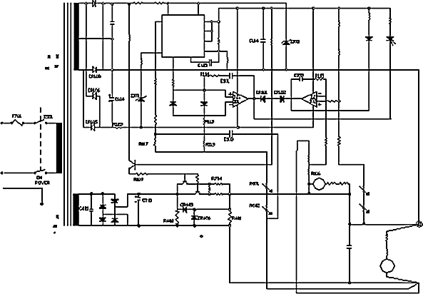
Component List
Resistors:
Resistor Values

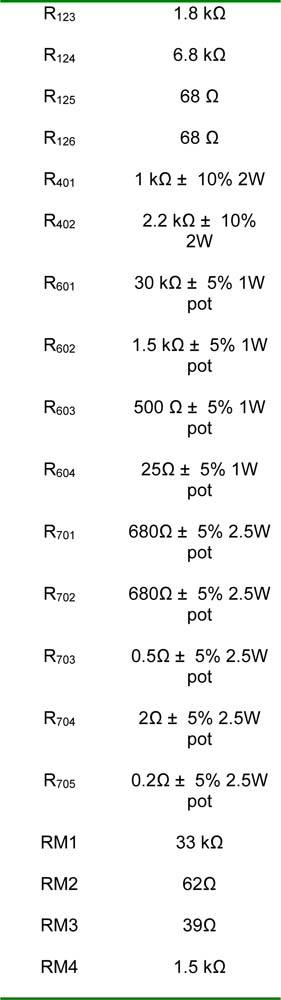
All resistors are ¼ W, ± 5% Carbon film unless otherwise specified.
Capacitor Values
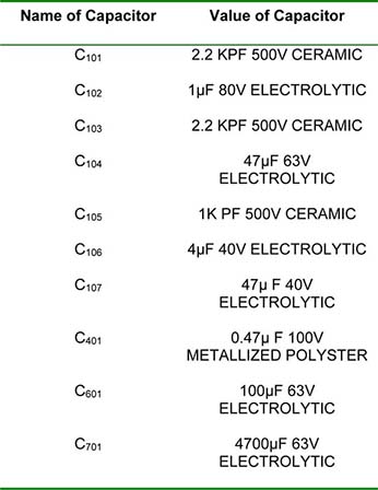
Diode Values
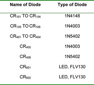
Zener Diode Values
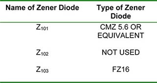
Transistor Values
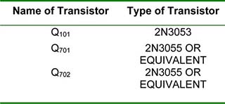
Integrated Circuits

Procedure:
For this exercise, a commercially available power supply is used. The following instructions can be suitably changed, based on the model used:
- Set all the control knobs to minimum position.
- Visually check all the components in the circuit whether they are as per the component list.
- Switch on the power supply. Inspect visually for abnormal behavior of any component
- Vary the voltage control knob. If the voltmeter provided in the equipment does not show any reading, connect a voltmeter externally.
- Vary the voltage control knob. If still there is no indication in the externally connected voltmeter, then refer to the following troubleshooting chart to identify the fault.
- If there is an indication of voltage variation in the external voltmeter, then check RM1 and RM2.
- Now, load the power supply to draw 1A current at 30V
- If there is no indication of current in ammeter provided in the equipment, then connect an ammeter externally. If there is still no indication of current, then again refer to the troubleshooting chart.
- If there is an indication of current in the external voltmeter, then check RM3 and RM4.
- Following is given the troubleshooting chart to identify the fault. After the fault is identified, the component can be replaced:
Troubleshooting Chart

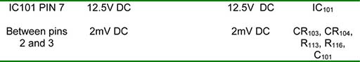
Conclusion:
The variable power supply (30V, 2A) was tested. The faults found during troubleshooting are (specify the faults).
The faults are rectified by (specify the action)
Professional Certificate of Competency in Advanced TCP/IP-Based Industrial Networking
Designed for engineers and technicians who need practical knowledge in…Read moreProfessional Certificate of Competency in Allen Bradley Controllogix / Logix5000 PLC Platforms
Designed for engineers and technicians who need practical knowledge in…Read moreProfessional Certificate of Competency in Arc Flash Protection
Designed for engineers and technicians who work in the electrical…Read moreProfessional Certificate of Competency in Chemical Engineering and Plant Design
Designed for engineers and technicians who need practical knowledge in…Read moreProfessional Certificate of Competency in Circuit Breakers, Switchgear and Power Transformers
Designed for engineers and technicians who need practical knowledge regarding…Read moreProfessional Certificate of Competency in Control Valve Sizing, Selection and Maintenance
Designed for engineers and technicians who need a solid understanding…Read moreProfessional Certificate of Competency in Electrical Power System Fundamentals for Non-Electrical Engineers
Designed for engineers and technicians who need to understand the…Read moreProfessional Certificate of Competency in Electrical Power System Protection
Designed for engineers and technicians who need practical skills and…Read moreProfessional Certificate of Competency in Electrical Wiring Standards: AS/NZS 3000:2018 (Australia and New Zealand Only)
This professional development course is designed for engineers and technicians…Read moreProfessional Certificate of Competency in Fundamental E & I Engineering for Oil and Gas Facilities
Designed for engineers and technicians who need to update their…Read moreProfessional Certificate of Competency in Gas Turbine Engineering
Designed for engineers and technicians who need practical skills in…Read moreProfessional Certificate of Competency in Hazardous Areas and Intrinsic Safety For Engineers and Technicians
Designed for engineers and technicians who need to understand the…Read moreProfessional Certificate of Competency in Heating, Ventilation and Air Conditioning (HVAC)
Designed for engineers and technicians from a wide range of…Read moreProfessional Certificate of Competency in IEC 61850 Based Substation Automation
Designed for engineers and technicians who need to understand the…Read moreProfessional Certificate of Competency in Industrial Data Communications
Designed for engineers and technicians who need to understand how…Read moreProfessional Certificate of Competency in Instrumentation, Automation and Process Control
Designed for engineers and technicians who need to gain practical…Read moreProfessional Certificate of Competency in Machine Learning and Artificial Intelligence
This professional development course is designed for engineers and technicians…Read moreProfessional Certificate of Competency in Mechanical Engineering
This professional development course is designed for engineers and technicians…Read moreProfessional Certificate of Competency in Onshore and Offshore Pipeline Systems
Designed for engineers and technicians who need to gain an…Read moreProfessional Certificate of Competency in Power Distribution
designed for engineers and technicians who need to gain a…Read moreProfessional Certificate of Competency in Practical Machine Learning Using Python for Engineers and Technicians
Designed to use Python Programming to work with machine learning…Read moreProfessional Certificate of Competency in Practical Python for Engineers and Technicians
Designed for engineers and technicians who need to understand the…Read moreProfessional Certificate of Competency in Programmable Logic Controllers (PLCs) & SCADA Systems
Designed for engineers and technicians who need to get practical…Read moreProfessional Certificate of Competency in Project Management for Engineers & Technicians
This professional development course is designed for engineers and technicians…Read moreProfessional Certificate of Competency in Safety Instrumentation Systems for Process Industries
Professional development course designed for engineers and technicians who want…Read moreProfessional Certificate of Competency in Sewage and Effluent Treatment Technologies
Designed for engineers and technicians who need practical skills and…Read moreProfessional Certificate of Competency in Structural Design for Non-Structural Engineers
Professional development course designed for engineers and technicians who need…Read moreProfessional Certificate of Competency in Substation Design (Main Equipment)
Professional development course is designed for engineers and technicians who…Read moreProfessional Certificate of Competency in Substation Design (Control, Protection and Facility Planning)
Designed for engineers and technicians who need to gain practical…Read moreProfessional Certificate of Competency in the Fundamentals of Process Plant Layout & Piping Design
Professional development course is designed for engineers and technicians who…Read moreProfessional Certificate of Competency in Practical Mechanical Sealing
This professional development course is designed for engineers and technicians…Read moreProfessional Certificate of Competency in Fundamentals of Road Construction
This professional development course is designed for engineers and technicians…Read moreProfessional Certificate of Competency in Specification and Technical Writing
Designed for engineers and technicians who need to understand how…Read moreProfessional Certificate of Competency in Hydraulics and Pneumatics
Overview of all aspects related to the construction, design, operation,…Read moreProfessional Certificate of Competency in Big Data and Analytics in Electricity Grids
This course explores the use of big data & data…Read moreProfessional Certificate of Competency in Renewable Energy Systems
This course covers various renewable energy systems that are popular…Read moreProfessional Certificate of Competency in Smart Grids
A smart grid is an electricity network that uses digital…Read moreProfessional Certificate of Competency in Hydrogen Energy – Production, Delivery, Storage, and Use
Hydrogen energy short course designed for engineers and professionals interested…Read moreProfessional Certificate of Competency in Earthing and Lightning Protection
Designed for engineers and technicians who need to understand the…Read moreProfessional Certificate of Competency in Building Information Modelling (BIM)
This professional development course is covering practical aspects of using…Read more


")


")


 & SCADA Systems")


")
")


")