")
52896WA Advanced Diploma of Civil and Structural Engineering (Materials Testing)
Investigation of the properties of construction materials, the principles which…Read more")
Graduate Diploma of Engineering (Safety, Risk and Reliability)
The Graduate Diploma of Engineering (Safety, Risk and Reliability) program…Read more
Professional Certificate of Competency in Fundamentals of Electric Vehicles
Learn the fundamentals of building an electric vehicle, the components…Read more
Professional Certificate of Competency in 5G Technology and Services Overview
Learn 5G network applications and uses, network overview and new…Read more
Professional Certificate of Competency in Clean Fuel Technology - Ultra Low Sulphur Fuels
Learn the fundamentals of Clean Fuel Technology - Ultra Low…Read more
Professional Certificate of Competency in Battery Energy Storage and Applications
Through a scientific and practical approach, the Battery Energy Storage…Read more
52910WA Graduate Certificate in Hydrogen Engineering and Management
Hydrogen has become a significant player in energy production and…Read more
Professional Certificate of Competency in Hydrogen Powered Vehicles
This course is designed for engineers and professionals who are…Read more
This manual will give you the tools to approach earthing and shielding issues in a logical and systematic way.
Practical Shielding, EMC/EMI, Noise Reduction, Earthing and Circuit Board Layout
Web Site: www.idc-online.com
E-mail: idc@idc-online.com
Copyright
All rights to this publication, associated software and workshop are reserved. No part of this publication or associated software may be copied, reproduced, transmitted or stored in any form or by any means (including electronic, mechanical, photocopying, recording or otherwise) without prior written permission of IDC Technologies.
Disclaimer
Whilst all reasonable care has been taken to ensure that the descriptions, opinions, programs, listings, software and diagrams are accurate and workable, IDC Technologies do not accept any legal responsibility or liability to any person, organization or other entity for any direct loss, consequential loss or damage, however caused, that may be suffered as a result of the use of this publication or the associated workshop and software.
In case of any uncertainty, we recommend that you contact IDC Technologies for clarification or assistance.
Trademarks
All terms noted in this publication that are believed to be registered trademarks or trademarks are listed below:
IBM, XT and AT are registered trademarks of International Business Machines Corporation. Microsoft, MS-DOS and Windows are registered trademarks of Microsoft Corporation.
Acknowledgements
IDC Technologies expresses its sincere thanks to all those engineers and technicians on our training workshops who freely made available their expertise in preparing this manual.
Who is IDC Technologies?
IDC Technologies is a specialist in the field of industrial communications, telecommunications, automation and control and has been providing high quality training for more than six years on an international basis from offices around the world.
IDC consists of an enthusiastic team of professional engineers and support staff who are committed to providing the highest quality in their consulting and training services.
The Benefits to you of Technical Training Today
The technological world today presents tremendous challenges to engineers, scientists and technicians in keeping up to date and taking advantage of the latest developments in the key technology areas.
- The immediate benefits of attending IDC workshops are:
- Gain practical hands-on experience
- Enhance your expertise and credibility
- Save $$$s for your company
- Obtain state of the art knowledge for your company
- Learn new approaches to troubleshooting
- Improve your future career prospects
The IDC Approach to Training
All workshops have been carefully structured to ensure that attendees gain maximum benefits. A combination of carefully designed training software, hardware and well written documentation, together with multimedia techniques ensure that the workshops are presented in an interesting, stimulating and logical fashion.
IDC has structured a number of workshops to cover the major areas of technology. These courses are presented by instructors who are experts in their fields, and have been attended by thousands of engineers, technicians and scientists world-wide (over 11,000 in the past two years), who have given excellent reviews. The IDC team of professional engineers is constantly reviewing the courses and talking to industry leaders in these fields, thus keeping the workshops topical and up to date.
Technical Training Workshops
IDC is continually developing high quality state of the art workshops aimed at assisting engineers, technicians and scientists. Current workshops include:
Instrumentation & Control
- Practical Automation and Process Control using PLC’s
- Practical Data Acquisition using Personal Computers and Standalone Systems
- Practical On-line Analytical Instrumentation for Engineers and Technicians
- Practical Flow Measurement for Engineers and Technicians
- Practical Intrinsic Safety for Engineers and Technicians
- Practical Safety Instrumentation and Shut-down Systems for Industry
- Practical Process Control for Engineers and Technicians
- Practical Programming for Industrial Control – using (IEC 1131-3;OPC)
- Practical SCADA Systems for Industry
- Practical Boiler Control and Instrumentation for Engineers and Technicians
- Practical Process Instrumentation for Engineers and Technicians
- Practical Motion Control for Engineers and Technicians
- Practical Communications, SCADA & PLC’s for Managers
Communications
- Practical Data Communications for Engineers and Technicians
- Practical Essentials of SNMP Network Management
- Practical Field Bus and Device Networks for Engineers and Technicians
- Practical Industrial Communication Protocols
- Practical Fibre Optics for Engineers and Technicians
- Practical Industrial Networking for Engineers and Technicians
- Practical TCP/IP & Ethernet Networking for Industry
- Practical Telecommunications for Engineers and Technicians
- Practical Radio & Telemetry Systems for Industry
- Practical Local Area Networks for Engineers and Technicians
- Practical Mobile Radio Systems for Industry
Electrical
- Practical Power Systems Protection for Engineers and Technicians
- Practical High Voltage Safety Operating Procedures for Engineers & Technicians
- Practical Solutions to Power Quality Problems for Engineers and Technicians
- Practical Communications and Automation for Electrical Networks
- Practical Power Distribution
- Practical Variable Speed Drives for Instrumentation and Control Systems
Project & Financial Management
- Practical Project Management for Engineers and Technicians
- Practical Financial Management and Project Investment Analysis
- How to Manage Consultants
Mechanical Engineering
- Practical Boiler Plant Operation and Management for Engineers and Technicians
- Practical Centrifugal Pumps – Efficient use for Safety & Reliability
Electronics
- Practical Digital Signal Processing Systems for Engineers and Technicians
- Practical Industrial Electronics Workshop
- Practical Image Processing and Applications
- Practical EMC and EMI Control for Engineers and Technicians
Information Technology
- Personal Computer & Network Security (Protect from Hackers, Crackers & Viruses)
- Practical Guide to MCSE Certification
- Practical Application Development for Web Based SCADA
Comprehensive Training Materials
Workshop Documentation
All IDC workshops are fully documented with complete reference materials including comprehensive manuals and practical reference guides.
Software
Relevant software is supplied with most workshop. The software consists of demonstration programs which illustrate the basic theory as well as the more difficult concepts of the workshop.
Hands-On Approach to Training
The IDC engineers have developed the workshops based on the practical consulting expertise that has been built up over the years in various specialist areas. The objective of training today is to gain knowledge and experience in the latest developments in technology through cost effective methods. The investment in training made by companies and individuals is growing each year as the need to keep topical and up to date in the industry which they are operating is recognized. As a result, the IDC instructors place particular emphasis on the practical hands-on aspect of the workshops presented.
On-Site Workshops
In addition to the quality of workshops which IDC presents on a world-wide basis, all IDC courses are also available for on-site (in-house) presentation at our clients premises.On-site training is a cost effective method of training for companies with many delegates to train in a particular area. Organizations can save valuable training $$$’s by holding courses on-site, where costs are significantly less. Other benefits are IDC’s ability to focus on particular systems and equipment so that attendees obtain only the greatest benefits from the training.
All on-site workshops are tailored to meet with clients training requirements and courses can be presented at beginners, intermediate or advanced levels based on the knowledge and experience of delegates in attendance. Specific areas of interest to the client can also be covered in more detail. Our external workshops are planned well in advance and you should contact us as early as possible if you require on-site/customized training. While we will always endeavor to meet your timetable preferences, two to three month’s notice is preferable in order to successfully fulfil your requirements. Please don’t hesitate to contact us if you would like to discuss your training needs.
Customized Training
In addition to standard on-site training, IDC specializes in customized courses to meet client training specifications. IDC has the necessary engineering and training expertise and resources to work closely with clients in preparing and presenting specialized courses.
These courses may comprise a combination of all IDC courses along with additional topics and subjects that are required. The benefits to companies in using training is reflected in the increased efficiency of their operations and equipment.
Training Contracts
IDC also specializes in establishing training contracts with companies who require ongoing training for their employees. These contracts can be established over a given period of time and special fees are negotiated with clients based on their requirements. Where possible IDC will also adapt courses to satisfy your training budget.
References from various international companies to whom IDC is contracted to provide on-going technical training are available on request.
Some of the thousands of Companies worldwide that have supported and benefited from IDC workshops are:
Alcoa, Allen-Bradley, Altona Petrochemical, Aluminum Company of America, AMC Mineral Sands, Amgen, Arco Oil and Gas, Argyle Diamond Mine, Associated Pulp and Paper Mill, Bailey Controls, Bechtel, BHP Engineering, Caltex Refining, Canon, Chevron, Coca-Cola, Colgate-Palmolive, Conoco Inc, Dow Chemical, ESKOM, Exxon, Ford, Gillette Company, Honda, Honeywell, Kodak, Lever Brothers, McDonnell Douglas, Mobil, Modicon, Monsanto, Motorola, Nabisco, NASA, National Instruments, National Semi-Conductor, Omron Electric, Pacific Power, Pirelli Cables, Proctor and Gamble, Robert Bosch Corp, Siemens, Smith Kline Beecham, Square D, Texaco, Varian, Warner Lambert, Woodside Offshore Petroleum, Zener Electric
Contents
1 Introduction 1
1.1 Introduction 1
1.2 EMI vs EMC 3
1.3 Interference sources 3
1.4 Need for standards 5
1.5 EMC – the issues 6
1.6 Electromagnetic disturbances 7
1.7 EMC testing categories 8
1.8 The compatibility gap 9
1.9 Emission, immunity and compatibility 10
1.10 Causes and consequences of EMI 11
1.11 Levels of compliance and EMC engineering application 12
2 EM principles 14
2.1 Introduction 14
2.2 Coupling paths: sources and victims 14
2.3 Coupling mechanisms 17
2.4 Coupling via the supply network 20
2.5 Electromagnetic fields 21
2.6 Rayleigh/Maxwell near/far fields 22
2.7 Coupling modes 23
2.8 Radiated emissions from PCB (differential mode) 24
2.9 Cable radiated emissions (common mode) 25
2.10 Coupling paths (conducted emissions) 26
2.11 Susceptibility to radiated field coupling 27
2.12 Transient sources 28
2.13 Automotive transients 29
2.14 Supply voltage phenomenon 30
3 EM principles – 2 32
3.1 Introduction 32
3.2 DM/CM conversion 32
3.3 Common mode rejection ratio (CMRR) 34
3.4 Units in EMC engineering 34
3.5 Spectrum usage and created Interference 36
3.6 Fourier analysis 37
3.7 Choice of logic family 39
3.8 Lightning and ESD bandwidth 39
4 Shielding 40
4.1 Introduction 40
4.2 Shielding and Murphy’s Law 41
4.3 LF magnetic shielding 43
4.4 Apertures and shielding effectiveness 43
4.5 Waveguides 44
4.6 Gasketting and sealing 45
4.7 Panel displays and keyboards 46
4.8 Ventilation and shielding 47
4.9 PCB-level shielding 49
5 Grounding 50
5.1 Introduction 50
5.2 Earth and safety ground 51
5.3 Grounding and frequency 53
5.4 Ground loops 54
5.5 Ground impedance 55
5.6 Ground topologies 55
5.7 Guidelines for grounding 57
6 Cables and connectors 60
6.1 Introduction 60
6.2 Cables in context 61
6.3 Cable parameters and implication 62
6.4 Cable types and frequency 62
6.5 Cable routing and screening 63
6.6 Types of screening 66
6.7 Screened and unscreened connectors 67
6.8 Transmission lines 69
6.9 Cable coupling to radiated field 71
6.10 Useful references 71
7 Circuits and components 72
7.1 Introduction 72
7.2 Parasitic in passives 73
7.3 Clocking 74
7.4 Choice of logic family 75
7.5 Design and component choice 75
7.6 Analog immunity and demodulation 76
8 Protection and filtering 80
8.1 Introduction 80
8.2 Filter types and operation 81
8.3 Soft ferrites 82
8.4 Thumb rules 83
8.5 Filter specifications 84
8.6 Impedance matching 85
8.7 Filtering precision and Filter earthing 86
8.8 Filters and shielding 87
8.9 Surge protection devices (SPDs) 88
8.10 Surge protection and data integrity 89
8.11 Surge protection ratings 90
8.12 Surge protection fusing 91
8.13 Positioning SPDs 92
8.14 Electrostatic discharge 93
8.15 Creepage and clearance 94
8.16 Shielding 95
8.17 Signal line protection 97
9 Engineering measurements 99
9.1 Introduction 99
9.2 Bench and test laboratory 99
9.3 Determining common mode noise 101
9.4 Field probes 103
9.5 Common mode and Differential mode currents 105
10 Power supplies 107
10.1 Introduction 107
10.2 PSUs as noise generators 108
10.3 Switch-mode PSU as a noise generator 109
10.4 Coupling paths, conducted emissions 109
10.5 Power supplies 110
10.6 Parasitic components in SMPS 110
10.7 Effects of diodes 111
10.8 Improvements from inductors 111
10.9 The mains filter 112
10.10 PSU threats 114
11 PCB design and layout 115
11.1 Introduction 115
11.2 Levels of EMC Engineering Application 116
11.3 PCB design objectives 117
11.4 Differential mode coupling 117
11.5 Common mode coupling 118
11.6 Electrical and physical parameters 119
11.7 Board layout 120
11.8 Component and track layout 120
11.9 Areas under control vs outside 121
11.10 Reference planes 122
11.11 The Image Plane effect 123
11.12 Maintaining plane integrity and gridded ground 124
11.13 Board layering 126
11.14 Layer stacking 126
11.15 Grounding on the board 129
11.16 0 V – Chassis Connection 131
11.17 Decoupling Capacitors 132
11.18 Transmission Lines on PCBs 134
11.19 Transmission line termination 135
11.20 Multiple boards and backplanes 136
11.21 Interfacing noisy and quite areas 136
12 EMC engineering management 137
12.1 Introduction 137
12.2 Why manage EMC? 137
12.3 Wait and its too late 139
12.4 How to manage EMC 139
12.5 Levels of compliance 141
12.6 EMC lifecycle 142
12.7 Life-cycle flow chart 143
12.8 EMC in context 144
12.9 How much effort? 144
12.10 Co-ordinating efforts 144
12.11 Design practices 145
12.12 EMC engineering implementation 145
12.13 Project management 146
12.14 Need for control plan 146
12.15 Test plans 147
12.16 Test reports (immunity) 149
12.17 Test and calibration of facilities 149
12.18 Maintaining EMC in production 150
13 Conclusion 151
13.1 Introduction 151
13.2 EMC Legalities 152
14 Tutorials 154
15 Practical Exercises 162
16 Powerpoint Slides 178
1.1 Introduction
Electromagnetic Compatibility (EMC) is defined as the ability of a device, equipment or a system to function satisfactorily in its electromagnetic environment without introducing intolerable electromagnetic disturbance to anything in that environment. Any electronic equipment is both capable of emitting unintended signals (i.e., interference to other electronic equipment) and also itself being affected by spurious radiation from other electronic equipment (i.e., interference caused by other electronic equipment). Putting these electronics together without affecting each other is the challenge. Meeting the challenge is a combination of legislation, engineering and consideration for the needs of others.
1.1.1 EMC – accepting the challenge!!!
Historically, EMC has been concerned principally with ensuring the proper operation of collections of electrical and electronic apparatus. Since interference is a function of separation distance, equipment used in close proximity to other equipment had to be compatible with its neighbors. Putting together a system out of several essentially different items of apparatus meant that these items were naturally close to each other, and their Electromagnetic Compatibility (EMC) was necessary in order for the system to work successfully. Hence the discipline of EMC grew up in those industry sectors where system integration was the norm. In the military, the majority of electrical and electronics equipment is used on platforms i.e., ships, aircraft and land vehicles, in their civilian equivalents, aerospace, rail, automotive and marine transport, and in the process control industry. The consumer, IT and professional equipment sectors largely escaped this discipline, because their individual products could assume a large enough separation distance that EMC could be regarded as a luxury rather than a necessity.
Commercial systems that faced issues of safety integrity had often to meet requirements for immunity from various phenomena such as radio frequency (RF) fields, electrostatic discharge (ESD), and various types of conducted transients. But these were contractual requirements, agreed between the equipment suppliers, and the system designers and operators. They were instigated as a result of operational experience, not because of legislation.
There is now an urgent need for mandatory measures to be taken to protect and ensure equipment EMC. Various national administrators have taken ad hoc measures in the past to impose restrictions on some of the electromagnetic properties of some types of products. These measures have often come to be seen as implementing back-door methods of protection, without the technical adequacy of some of the requirements allowing effectively different standards to be applied to imported and indigenous products. In an effort to recognize the need for EMC protection measures and at the same time to eliminate the protectionist barrier to trade throughout the European Community, the European Commission adopted in 1989 a Directive on the approximation of the laws of the Member States relative to electromagnetic compatibility, otherwise known as the EMC Directive.
At times, EMC problems and their solutions do seem like black magic rather than engineering. Here are few of the examples?
- This is an instance from the Falklands war: HMS Sheffield turned off its missile warning RADAR because it interfered with the satellite communication system of the ship. The result of this was – HMS Sheffield was sunk by an enemy missile, which could otherwise have been detected.
- An engineering company installed a CAD system to speed up design time. However, the system crashed so often that they were falling even further behind. Numerous calls to the suppliers failed to solve the problem that everyone thought was software-related. Investigation showed eventually that a large drawing reproduction machine that injected transients onto the mains supply caused it.
- In February ’99, while approaching JFK airport, a DC 10 passenger airplane banked hard left all by itself, almost crashing. The cause of it was suspected to be a CD player being played in 1st class.
- Much of the bad press surrounding CD players and aircraft seems to have originated with a Lufthansa flight where a system operating at 112 MHz had problems which were traced to a CD player with a clock rate of 28 MHz. The system operating frequency is equal to 4 times the clock rate of the CD player.
- A paper mill in Stanger (South Africa) was experiencing trips on its 1 MVA variable speed drive system. A voltage dip of 20%, lasting for more than 40 ms was enough to trip the system and would result in several hours of downtime while the paper web was re-threaded and the system started up again. Installation of a SMES (Superconducting Magnetic Energy Storage System) has meant that there have been no further system trips since 1997.
- In an aerospace factory, a plastic welder was being operated quite legally. Nearby is a mattress factory. Although both are tens of meters away from each other, the welder caused a mattress to burst into flames.
Here is a statement (which may sound familiar) given by the past chairman of the Scottish branch of the Institute of Structural Engineers ‘… the art of modelling materials we do not understand, into shapes we cannot precisely analyse, to withstand forces we cannot properly assess, in such a way that the public at large has no reason to suspect the extent of our ignorance’.
In this workshop, we will be looking at engineering ways to prevent and solve EMC problems without the need for witches, wizards and other supernatural means.
1.2 EMI vs EMC
Electromagnetic interference (EMI) is a serious and increasing form of environmental pollution. Its effects range from extremely small annoyances due to crackles on broadcast reception, to potentially fatal accidents due to corruption of safety-critical control systems. Various forms of EMI may cause electrical and electronic malfunctions, can prevent the proper use of the radio frequency spectrum, can ignite flammable or other hazardous atmospheres, and may even have a direct effect on human tissue. As electronic systems penetrate more deeply into all aspects of society, so both the potential for interference effects and the potential for serious EMI-induced incidents will increase.
The threat of EMI is controlled by adopting the practices of electromagnetic compatibility (EMC). The term EMC has two complementary aspects:
- It describes the ability of electrical and electronic systems to operate without interfering with other systems
- It also describes the ability of such systems to operate as intended within a specified electromagnetic environment
Thus it is closely related to the environment within which the system operates. Effective EMC requires that the system is designed, manufactured and tested with regard to its predicted operational electromagnetic environmental (i.e., the totality of electromagnetic phenomena existing at its location). Although the term electromagnetic tends to suggest an emphasis on high frequency field-related phenomena, in practice the definition of EMC encompasses all frequencies and coupling paths, from DC through mains supply frequencies and microwaves.
1.3 Interference sources
Devices that cause continuous noise
There are two types of internal and external interference, viz., continuous and intermittent. Each type has its own cause.
Continuous interference
Continuous, or Continuous Wave (CW), interference arises where the source continuously emits at a given range of frequencies. This type is naturally divided into sub-categories according to frequency range, and as a whole is sometimes referred to as “DC to daylight”.
- Audio Frequency, from very low frequencies up to around 20kHz. Frequencies up to 100kHz may sometimes be classified as Audio. Sources include:
- Mains hum from: power supply units, nearby power supply wiring, transmission lines and substations.
- Audio processing equipment, such as audio power amplifiers and loudspeakers.
- Demodulation of a high-frequency carrier wave such as an FM radio transmission.
- Radio Frequency Interference (RFI), from typically 20kHz to an upper limit which constantly increases as technology pushes it higher. Sources include:
- Wireless and Radio Frequency Transmissions
- Television and Radio Receivers
- Industrial, scientific and medical equipment (ISM)
- Digital processing circuitry such as microcontrollers
- Broadband noise may be spread across parts of either or both frequency ranges, with no particular frequency accentuated. Sources include:
- Solar activity
- Continuously operating spark gaps such as arc welders
- CDMA (spread-spectrum) mobile telephony
Pulse or transient interference
An electromagnetic pulse (EMP), sometimes called a transient disturbance, arises where the source emits a short-duration pulse of energy. The energy is usually broadband by nature, although it often excites a relatively narrow-band damped sine wave response in the victim.
Sources divide broadly into isolated and repetitive events.
- Sources of isolated EMP events include:
- Switching action of electrical circuitry, including inductive loads such as relays, solenoids, or electric motors.
- Electrostatic discharge (ESD), as a result of two charged objects coming into close proximity or contact.
- Lightning electromagnetic pulse (LEMP), although typically a short series of pulses.
- Nuclear electromagnetic pulse (NEMP), as a result of a nuclear explosion. A variant of this is the high altitude EMP (HEMP) nuclear device, designed to create the pulse as its primary destructive effect.
- Non-nuclear electromagnetic pulse (NNEMP) weapons.
- Power line surges/pulses
- Sources of repetitive EMP events, sometimes as regular pulse trains, include:
- Electric motors
- Gasoline engine ignition systems
- Continual switching actions of digital electronic circuitry.
It is also possible to categorise the different types of EMI by their bandwidth.
- Narrowband: Typically this form of EMI is likely to be a single carrier source – possibly generated by an oscillator of some form. Another form of narrowband EMI is the spurious signals caused by intermodulation and other forms of distortion in a transmitter such as a mobile phone of Wi-Fi router. These spurious signals will appear at different points in the spectrum and may cause interference to another user of the radio spectrum. As such these spurious signals must be kept within tight limits.
- Broadband: There are many forms of broadband noise which can be experienced. It can arise from a great variety of sources. Man-made broadband interference can arise from sources such as arc welders where a spark is continuously generated. Naturally occurring broadband noise can be experienced from the Sun – it can cause sun-outs for satellite television systems when the Sun appears behind the satellite and noise can mask the wanted satellite signal. Fortunately these episodes only last for a few minutes.
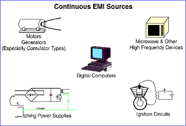
The most common causes of continuous interference are:
- 50/60 Hz Supply Power
- Electric Motor (Especially Commutator Type)
- High Power Radio Signals
- Switch Mode Power Supplies
- Microwave Ovens
- Ignition Circuits
Devices that cause constant noise emissions are usually easier to find than intermittent noise problems. This is because the noise doesn’t go away while the system is being looked at. The most common constant noise source is hum, caused by a 50/60 Hz supply power. Supply power is the most common noise component because it is an oscillating voltage, has high power and has a huge antenna system. Almost every system has some form of power filtering for 50/60 Hz supply power. This filtering can take the form of either trying to keep 50/60 Hz noise from getting into our device or leaving the device.
High power electric motors often create wideband noise. They can radiate noise into almost any equipment that is in close proximity to the motor. DC motors often have switch mode power supplies that cause high frequency noise through the common power ground. As motors ramp up and down the noise can vary in frequency and power. This wideband motor noise can then be transmitted back through the power supply lines or through a common earth ground.
Local radio, television stations, radar and ham radio stations can cause radio frequency noise. Military radar is the highest power radio system, but TV, AM and FM local radio stations are usually more common. These stations put out kilowatts of power and often are relatively close to industrial areas.
Switch mode power supplies are fast becoming the most common noise source of all. This is because they are so popular as a low voltage plug pack in home electronics. They create large amounts of harmonic frequencies. The power supplies develop low voltages from mains power by switching the high voltage on and off very quickly that creates lots of noise. The wires that connect the power supply to the device then transmit this noise. Switch mode power supplies are very popular because they are not frequency or voltage dependent and can be used in any country and on almost any device.
Microwave ovens radiate wideband noise by leakage through edges of the door or from the power supply wires. The oven can transmit hundreds of watts over short distances. While this is good for cooking the food, it also can create life-threatening situations for people with pacemakers. Ignition circuits in motorcycles, cars and other gasoline powered motors put out wideband noise created by tens of thousands of Volts. Most automobiles have some sort of suppression circuit, but if this fails it can cause havoc with it’s own electronics and nearby devices. Older motorcycles, lawn mowers and other simple engines often have little or no noise suppression and therefore emit large amounts of noise.
Devices that cause intermittent wideband noise are:
- Lightning
- Switching Relay Equipment
- Arc Welding
- Static

Devices that cause intermittent noise
Intermittent noise components are often hard to find. There is an old saying in electronics… If it’s not broke, it can’t be fixed. And since the noise comes and goes the problem is usually only present part of the time.
Lightning can be the most damaging of the intermittent noise. A typical lightning strike can contain 20 to 40 thousand Amps and millions of Volts. In addition, the lightning strike transmits wideband noise that covers the whole frequency spectrum from DC to X-rays. This, in conjunction with the high current and voltage, makes it impossible to filter out lightning noise. The best method is to keep the lightning away from the circuit by using protection devices like shunts and suppressors.
Turning off relays usually causes relay switching noise. This noise is created by the magnetic field collapsing when the relay is turned off. This type of noise is common in industrial environments.
Arc welding is man-made lightning and has all the attributes of lightning such as high current, high voltage and wideband frequency noise. The advantage here is that it is often very intermittent and can be easily recognized.
Static is very hard to prove as a noise source as it is often invisible and very intermittent. Although is often man-made, it can be natural in origin. Equipment can be spiked by static build up in the air as well as from a person. Static noise is also very similar to lightning with all the same attributes except on a smaller scale.
1.4 Need for standards
Standards are required to control interference from the electronic devices, i.e., to make electronic devices less susceptible to interference. Various countries implemented their own standards, some of the standards are as mentioned below:
- IEC (International Electrotechnical Commission) – the IEC operates in close co-operation with the International Organization (ISO). It is composed of National Committees that are expected to be fully representative of all electrotechnical interests in their respective countries. Two IEC technical committees are devoted full time to EMC work is TC77, Electromagnetic compatibility between equipment including networks, and the International Special Committee on Radio Interference or CISPR.
- CENELEC (European Committee for Electrotechnical Standardization) and ETSI (European Telecommunications Standards Institute) – CENELEC is the European standards making body, which has been mandated by the Commission of the EC (European Commission) to produce EMC standards for the use with European EMC Directive. For Telecommunications equipment ETSI is the mandated standards body. ETSI generates standards for telecom network equipment that is not available to the subscriber, and for the radio communications equipment and broadcast transmitters.
Any manufacturer wanting to market his/her goods into a particular country has to comply with the standards followed by that country.
1.5 EMC – the issues
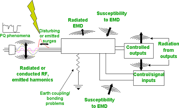
EMC issues
Figure 1.3 shows the EMC issues in a diagrammatic way. Any electronic device will emit radiation in the form of –
- Radiated RF electromagnetic disturbances from the device itself
- Radiated RF electromagnetic disturbances from its input and output connections
- Conducted EMD via its I/O connections or power lines
Any electronic device will be susceptible to EMD from –
- Stray radiation from other electronic equipment
- Stray radiation from the I/O of other electronic equipment
- Conducted disturbances via mains lines or I/O, or
- Mains voltage variations or waveshape
1.6 Electromagnetic disturbances
Any electromagnetic phenomenon may degrade the performance of the system. Some of the electromagnetic issues are as mentioned below:
Voltage fluctuations: short-term (sub-second) fluctuations with quite small amplitudes are annoyingly perceptible on electric lightning, though electronic power supply circuits comfortably ignore them. Generation of flicker by high power load switching is subject to regulatory control.
Waveform distortion: at source, the AC mains is generated as a pure sine wave but the reactive impedance of the distribution network together with the harmonic currents drawn by non-linear loads causes voltage distortion. Power converters and electronic power supplies are important contributors to non-linear loading. Harmonic distortion may actually be worse at points remote from the non-linear load because of resonance in the network components. Not only must non-linear harmonic currents be limited but also equipment should be capable of operating with up to 10% total harmonic distortion in the supply waveform.
Voltage variations: the distribution network has finite source impedance and varying loads will affect the terminal voltage. Not including voltage drops within the customer’s premises, an allowance of ±10%, on the nominal voltage will cover normal variations in the UK. The effect of the shift in nominal voltage from 240 V to 230 V, as required by CENELEC Harmonization Document HD 472 S1: 1988 and implemented in the UK by BS 7697: 1993, is that from 1st January 1995 the UK nominal voltage is 230 V with a tolerance of +10%, –6%. After 1st January 2003 the nominal voltage will be 230 V with a tolerance of ±10%, in the line with all other Member States.
Transients and surges: switching operations generate transients of a few hundred volts as a result of current interruption in an inductive circuit. These transients normally occur in bursts and have risetimes of no more than a few nsec, although the finite bandwidth of the distribution network will quickly attenuate all but local sources. High amplitude spikes in excess of 2 kV may be observed due to fault conditions. Even higher voltage surges due to lightning strikes occur – mostly on exposed overhead line distribution systems in rural areas.
Voltage interruptions: faults on power distribution systems cause almost 100% voltage drops but are cleared quickly and automatically by protection devices, and throughout the rest of the system the voltage immediately recovers. Most consumers therefore see a short voltage dip. The frequency of occurrence of such dips depends on location and seasonal factors.
- Supply voltage – Mains electricity suffers a variety of disturbing effects during its distribution. These may be caused by sources in the supply network or by other users, or by other loads within the same installation. A pure, uninterrupted supply would not be cost effective; the balance between the cost of the supply and its quality is determined by national regulatory requirements, tempered by the experience of the supply utilities. Typical disturbances are:
- # Interruptions
- # Dips
- # Surges
- # Waveform distortion
- # Fluctuations
- # Voltage imbalance
- # Frequency variations
- # DC in AC networks
- # Power-line carrier signaling
- Transient overvoltages – transient overvoltages on supply, signal and control lines that may occur because of lightning, switching or ESD (electrostatic discharge) can degrade the system performance. Take an example of an EMC phenomenon caused because of an ESD transient. An ESD transient can corrupt the operation of a microprocessor or clocked circuit just as a transient coupled into the supply or a signal port.
- Radio frequency fields – radio frequency fields, pulsed (radar), modulated and continuous, coupled directly into the equipment or onto its connected cables, may also degrade the system performance to a great extent.
- NEMP (nuclear electromagnetic pulse) – this is the effect of a high altitude nuclear explosion, which generates a sub-nanosecond nuclear electromagnetic pulse (NEMP) that is disruptive over an area of hundreds of square kilometers.
- LF magnetic or electric fields
1.7 EMC testing categories
Figure 1.4 shows the diagrammatic view of the EMC testing categories. The four categories are as follows:
- Conducted Emission (CE)
- Conducted Susceptibility (CS)
- Radiated Emission (RE)
- Radiated Susceptibility (RS)

EMC testing categories
All electronic devices are susceptible to electromagnetic disturbances, if it is not the case, then there would be no EMC issue. However, none of the electronic devices are completely immune and so the EMC problem still exists. Electromagnetic Susceptibility can be defined as the inability of a device, equipment or a system to perform without degradation in the presence of an electromagnetic disturbance. On the other hand, immunity to electromagnetic disturbances can be defined as the ability of a device, equipment or a system to perform without degradation in the presence of an electromagnetic disturbance.
1.8 The compatibility gap
The increasing susceptibility of electronic equipment to electromagnetic influence is being paralleled by an increasing pollution of the electromagnetic environment. Susceptibility is a function of the adoption of VLSI technology in the form of microprocessors, both to achieve new tasks and for those that were previously tackled by electromechanical or analog means, and the accompanying reduction in the energy required of potentially disturbing factors. It is also a function of the increased penetration of radio communications, and the greater opportunities for interference to radio reception that result from the co-location of unintentional emitters and radio receivers.
At the same time more radio communications means more transmitters and an increase in the average RF field strengths to which equipment is exposed. Also, the proliferation of digital electronics means an increase in low-level emissions that affect radio reception – a phenomenon that has been aptly described as a form of electromagnetic smog. Only legislation to limit the effects of interaction can solve the problem.
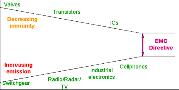
Compatibility gap
These concepts can be graphically presented in the form of a narrowing electromagnetic compatibility gap, as shown in Figure 1.5. This gap is of course conceptual rather than absolute, and the phenomena defined as emissions and those defined as immunity do not mutually interact except in rare cases. But the maintenance of some artificially-defined gap between equipment immunity and radio transmissions on the other hand, and equipment emissions and radio reception on the other, is the purpose of the application of EMC standards, and is one result of the enforcement of the EMC directive.
1.9 Emission, immunity and compatibility
Relation between emission, immunity and compatibility is as shown by graphical representation in Figure 1.6. As shown in the Figure, there are 3 different levels:
- The lowermost level is the Emission level; the maximum level in emission level is the emission limit. The emissions from the devices should be within this level and it should not exceed the emission limit.
- The uppermost level is the Immunity level; the minimum level in the immunity level is the immunity limit. The immunity of the devices should be within this level and it should not be less than the immunity limit.
- The middle level is the Compatibility level; the difference between the Immunity limit and the Emission limit is the Compatibility Margin. Greater the compatibility margin, lesser the chances of EMC problems.
For proper functioning of a system, the devices should be compatible (with respect to EM environment) and hence the term Compatibility.
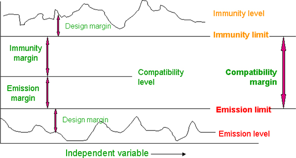
Emission, Immunity and Compatibility
1.10 Causes and consequences of EMI
The consequences of EMI can be classified in different categories depending on its criticality. Some of the causes of EMI that results into these consequences are mentioned below:
- Malfunction of a safety-critical item of machinery
- Erratic operation of moving equipment
- A safety device to ignore a signal
- An operation to stop for no apparent reason
- Not carry out its intended function, but not cause any havoc as a result
The malfunction will fall into the below mentioned classifications depending on the type of damage or loss occurred.
- Catastrophic – death, major injuries, downstream consequences
- Critical – minor injuries, extensive damage
- Major – minor permanent damage
- Minor – temporary performance loss
- Inconsequential – loss of performance within tolerance, no human intervention needed
1.10.1 Test result classification
For an item of equipment to pass a test, the test result must be determined beforehand. An important part of achieving compliance with any regulation is that the specification details what will happen under EMI conditions. The test result can be classified as follows:
- Normal performance within specified limits
- Self-recoverable temporary degradation or loss of function
- Temporary degradation or loss of function that requires human intervention or system reset
- Degradation or loss of function due to physical damage; software or data corruption
1.11 Levels of compliance and EMC engineering application
1.11.1 Levels of compliance
There are different levels of EMC engineering. Figure 1.7 shows the compliance structure showing different levels at which designers and companies operate.
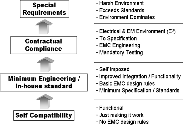
Levels of compliance
The four levels of compliance are as follows:
- Self-compatibility
- Minimum engineering/in-house standard
- Contractual compliance
- Special requirements
The above is useful to appreciate the change in engineering strategy – say a company was just struggling to make things works, but must now it must comply with specifications.
1.11.2 Levels of EMC engineering application
This course aims to equip with tools to design for and reduce EMI. Three main areas of application will be dealt with:
- PCBs
- Circuits/filters
- Screening
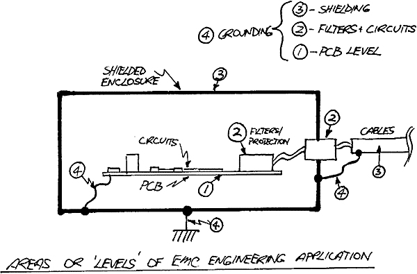
Levels of EMC Application Engineering
Proper grounding is underlying to all of the above areas and is also dealt with. Figure 1.8 shows the different areas.
PCBs can be seen as the inner or primary line of defence. The circuits on PCBs are where EMI problems eventually start and end. Proper PCB layout is the most subtle and cost effective way of influencing EMI. It controls EMI coupling right at the source or receptor – the circuit.
Filters and special circuits are used around the inner PCB as a secondary control measure or line of defence. When a PCB layout only does not eliminate unwanted interference, extra circuits and filters are added. Extra circuits imply more real estate and costs. Protection devices and circuits fall into this category.
Shielding is the tertiary or outer line of defence. This includes cables, screens and enclosures. If both of the above areas of application do not suffice, shielding is needed. The least cost effective solution and sometimes a last brute force attempt at compliance.
The fourth area of application (although not a level) is grounding. It determines the effectiveness and way all three levels interact. Grounding is applicable to all three of the above areas. Grounding on PCB level between different types of circuits is crucial. Filters/protection do not work properly if poorly grounded. Grounding of cable screens and enclosures has a primary influence on its shielding effectiveness.
2.1 Introduction
Electromagnetic interference (EMI) is caused in the presence of two parties, viz., a source and a victim. The source of interference is the aggressive circuits. High speed, noisy or dirty circuits come under the category of aggressive circuits. These are the noise generating circuits that also cause interference. The victims are sensitive circuits that are susceptible to interference. Sensitive, clean and quiet circuits come under the category of victim circuits. Any electronic device has the potential to radiate or conduct emission, and at the same time, they themselves are susceptible to it. In some cases, a victim itself acts as a source of interference. It is very important to understand which of the circuits (or modules) come under the category of ‘source’ and/or ‘victim’. Understanding such a mechanism helps in solving EMC problems.
2.2 Coupling paths: sources and victims
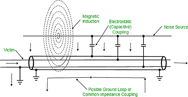
Figure 2.1 shows the potential interference routes that exist from one to the other when source and victim are put together. When the systems are built, it is necessary to know the emission signature and susceptibility of the component (equipment), along with problems that are likely to be experienced with close coupling. Following the published emission and susceptibility standards does not ensure freedom from system EMC problems. Standards are written for protecting a particular service, in the case of emissions, these are radio broadcast and telecommunications – they have to assume a minimum separation distance between source and victim. Most electronic devices consist of elements that are capable of antenna-like behaviour (i.e., they tend to radiate) such as cables, PCB tracks, internal wiring and mechanical structures. These elements can unintentionally transfer energy in the form of either electric, magnetic or electromagnetic fields that couple with the circuits. In practical situations, intra-system and external coupling between equipment is generally modified by the presence of screening and dielectric materials, and by the layout and proximity of interfering and victim equipment and especially their respective cables. Ground or screening planes tend to enhance interfering signal by reflection or attenuate it by absorption. Cable-to-cable coupling can be either inductive or capacitive and it depends on orientation, length and proximity. In most practical situations, dielectric materials may also reduce the field by absorption, though this is negligible compared to the effects of conductors.
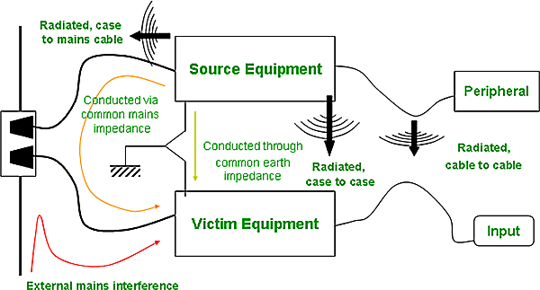
Coupling paths: sources and victims
2.2.1 Universal interference model

Universal interference model
Figure 2.2 shows the working of EMI in the form of Universal Interference Model. It shows that there is always a noise source (i.e., culprit), receptor (i.e., victim) and coupling path (i.e., interference path).
The solution for reducing interference can be at the source, receptor or coupling path. The following are the means the reduce interference:
- Remove or reduce noise at source – low noise design, shielding, decoupling, etc.
- Improve victim immunity – high immunity design, shielding, filtering, decoupling, etc.
- Remove or attenuate coupling path – isolation, re-routing, shielding, spacing, filtering, etc.
2.2.2 Noise sources
Noise sources are present everywhere, some of the sources of noise are as mentioned below:
- RF Transmitters – anything that generates RF are the sources of noise. Telemetry, Mobile phones, Radar, X-ray equipment, etc. are the applications that generates RF energy.
- Receivers – anything that has PLL (Phase Locked Loop) or clock are sources of noise. Local Oscillators, Computer and Peripherals come under this category.
- Anything that switches current is source of noise. Equipments such as Motors, SMPS (Switch Mode Power Supply), Power Lines, Engine Ignition, Fluorescent Lights, etc. come under this category.
- Anything that causes Arc is source of noise. Arc Welders, Motors, Relays, etc. come under this category.
- Natural – Galastic Noise, Lightning, Atmospheric noise, etc. are also the sources of noise.
2.2.3 Receptors
Receptors are present everywhere and some of the victims (receptors) are as mentioned:
- Anything intended for RF reception or using tuned circuits may be victims. Telemetry Receivers, Radar, etc. are victims to noise.
- Anything that can be disturbed by shifting logic levels, timing or clock disturbances, memory or data line toggling, etc. Digital electronics, software, etc. fall under this category.
- Any sensitive circuit such as Analog electronics that can amplify, rectify, saturate, shift levels, etc. are victims.
- Sensitive materials like Fuel, Ammunition that has risk of burning, exploding also proves victims to noise.
- Biological hazards to human beings (in this case, human beings are victims).
2.2.4 Coupling media
The below mentioned are the considerations to be made while changing the coupling between source and victim.
- Space separation
- Shielding materials
- Absorptive materials
- Cables
- Ground inter coupling
- Filters and circuits
- Power lines
2.3 Coupling mechanisms
There are many ways in which the electromagnetic interference can be coupled from the source to the receiver. Understanding which coupling method brings the interference to the receiver is key to being able to address the problem.
- Radiated: This type of EMI coupling is probably the most obvious. It is the type of EMI coupling that is normally experienced when the source and victim are separated by a large distance – typically more than a wavelength. The source radiates a signal which may be wanted or unwanted, and the victim receives it in a way that disrupts its performance.
- Conducted : Conducted emissions occur as the name implies when there is a conduction route along which the signals can travel. This may be along power cables or other interconnection cabling. The conduction may be in one of two modes:
- Common mode: This type of EMI coupling occurs when the noise appears in the same phase on the two conductors, e.g. out and return for signals, or +ve and -ve for power cables.
- Differential mode: This occurs when the noise is out of phase on the two conductors.
- The filtering techniques required will vary according to the type of EMI coupling experienced. For common mode lines are filtered together. For differential mode they may be filtered together.
- Inductive coupling: What is normally termed inductive coupling can be one of two forms, namely capacitive coupling and magnetic induction.
- Capacitive coupling : This occurs when a changing voltage from the source capacitively transfers a charge to the victim circuitry.
- Magnetic coupling: This type of EMI coupling exists when a varying magnetic field exists between the source and victim – typically two conductors may run close together (less than λ apart). This induces a current in the victim circuitry, thereby transferring the signal from source to victim.
By determining the form of coupling that exists and the way in which it is reaching the victim, it may prove to be that the most effective method of reducing the EMI is by putting measures in place to reduce the coupling and reduce the level of interference to an acceptable level.
Electromagnetic interference, EMI is present in all areas of electronics. By understanding the source, the coupling methods and the susceptibility of the victim, the level of interference can be reduced to a level where the EMI causes no undue degradation in performance.
Any EMI problem will involve any or a combination of the below mentioned coupling mechanism.
- Common impedance (Conducted)
- Capacitive (Electrostatic)
- Inductive (Magnetic)
- Electromagnetic (Radiated)
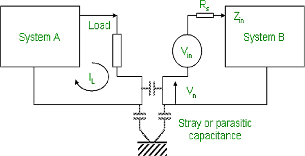
2.3.1 Common impedance (conducted)
From Figure 2.3, when an interference source (i.e., output of system A) shares a ground connection with a victim (i.e., input of system B) then any current due to A’s output flowing through the common impedance section (denoted by inductance L in Figure 2.3) develops a voltage in series with B’s input. The common impedance need not be more than a length of wire or pcb track, but high frequency or high di/dt components in the output will couple more efficiently because of the inductive nature of the impedance. The voltage developed across an inductor as a result of current flow through it is given by the equation 1 below:
V = –L×dIL/dt …………….(1)
where, L is the self inductance in H (Henries).
The output and input may be part of the same system; in this case there is a spurious feedback path through the common impedance that can cause oscillation. The solution as shown in Figure 2.3 is to simply re-route the connections so that there is no common current path, and hence no common impedance between the two circuits. The only penalty for doing this is the requirement for extra wiring or track to define the separate circuits. This applies to any circuit that may include common impedance (such as power rail connections). Grounds are most usual source of common impedance because the ground connection (generally not shown on circuit diagrams) is often taken for granted.

Conductive connection (common mode coupling)
2.3.2 Inductive (magnetic)

Magnetic induction
AC current flowing in a conductor creates a magnetic field that will couple with a nearby conductor and induce a voltage in it as shown in Figure 2.4. The voltage induced in the victim conductor is now given by equation 2 below:
Vn = –M×dIL/dt …………….(2)
where, M is mutual inductance in H (Henries).
Notice the similarity between equation 2 and equation 1; M depends on the areas of the source and victim current loops, their orientation and separation distance, and the presence of any magnetic screening. Whether or not there is a direct connection between the two circuits, the coupling remains unaffected; the induced voltage would be the same even if the circuits were isolated or connected to ground.
2.3.3 Capacitive (electrostatic)
Electrostatic coupling
Changing voltage on one conductor creates an electric field that may couple with a nearby conductor and induce a voltage on it, as shown in Figure 2.5. The voltage induced on the victim conductor is given by equation 3 below:
Vn = CC × dVL/dt × Zin//RS …………….(3)
where, CC is the coupling capacitance,
Zin//RS is the impedance to ground of the victim circuit.
This assumes that the impedance of the coupling capacitance is much higher than that of the circuit impedances. The noise is injected as if from a current source with a value of CC . dVL/dt. The value of CC is a function of the distance between the conductors, their effective areas and the presence of any electric screening material.
2.3.4 Real world coupling
A combination of coupling mechanisms exists in the real world. One type of coupling can dominate, but sometimes a combination is present as shown in Figure 2.6.
Real world coupling
2.3.5 Mutual C and L vs Lead Spacing
Both mutual capacitance and inductance are affected by the physical separation of the source and victim conductors. Figure 2.7 is the graph showing the effects of the spacing between conductors on their ability to couple from one circuit to another.

Mutual capacitance and inductance V/s Lead spacing
2.4 Coupling via the supply network
Propagation of interference from a source to a victim can take place via the mains distribution network to which both are connected. This is not well characterized at high frequencies, since the electrical loads connected can present virtually any RF impedance at their point of connection. From Figure 2.8 we can see that the RF impedance presented by the mains can approximate a network of 50 Ω in parallel with 50 μH on the average. For short distances (such as that between adjacent outlets on the same ring) coupling via the mains connection of two items of equipment can be represented by the Figure 2.8.
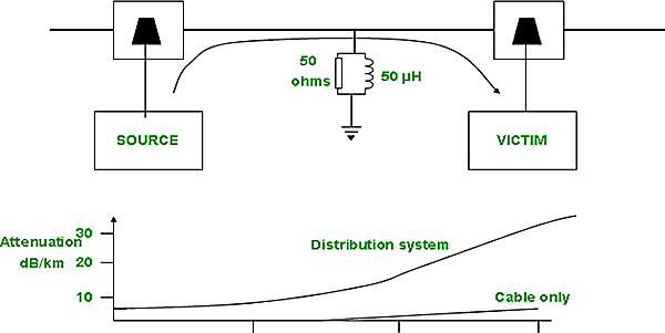
Coupling via the supply network
Over longer distances, power cables are fairly low loss transmission lines having characteristic impedance of about 150-200 Ω up to about 10 MHz. However, in any local power distribution system the disturbances and discontinuities introduced by load connections, cable junctions and distribution components dominates the RF transmission characteristic, in turn these all tends to increase the attenuation.
2.5 Electromagnetic fields
Two conductors at different potentials generate an electric field (E field) between them. The field is proportional to the applied voltage divided by the distance between the conductors and is measured in volts per meter (V/m).
A conductor carrying a current generate magnetic field (H field) around it. The field is proportional to the current divided by the distance from the conductor and is measured in amps per meter (A/m).
When an alternating voltage generates an alternating current through a network of conductors (this description applies to any electronic circuit), an electromagnetic (EM) wave is generated that propagates as a combination of E and H fields. The speed of propagation of EM wave is determined by the medium (in free space it is equal to the speed of light, i.e., 3×10⁸ m/s). Near to the radiating source, the geometry and strength of the fields depend on the characteristics of the source. A circuit node carrying a significant dv/dt (rate of change of voltage) will generate mostly an electric field; a conductor carrying a significant di/dt (rate of change of current) will generate mostly a magnetic field. The structure of these generated fields will be determined by the physical layout of the source conductors, as well as by other conductors, dielectrics and permeable materials in the vicinity. Further away from the source, the complex three-dimensional field structure decays and only the components that are orthogonal to each other and to the direction of propagation remain. Figure 2.9 demonstrates these ideas graphically.

Electromagnetic fields
2.6 Rayleigh/Maxwell near/far fields

Wave Impedance, and Rayleigh and Maxwell distances for transition to far field
The ratio of the electric to magnetic field strengths (i.e., E/H) is called the wave impedance (Figure 2.10). The wave impedance is a key parameter of any given wave as it determines the efficiency of coupling with another conducting structure, and also the effectiveness of any conducting screen that is used to block it. Radiated emissions can be divided into near field and far field.
In the far field, i.e., for d > λ/2π, the wave is known as a plane wave and the E and H fields decline with distance at the same rate. Therefore its impedance is constant, and is equal to the impedance of free space given by equation 4:
Zo = √μo/ɛo = 120π = 377 Ω …………….(4)
where, μo = 4π . 10-7 H/m, permeability of free space
ɛo = 8.85 . 10-12 F/m, permittivity of free space
In the near field, i.e., for d < λ/2π, the wave impedance is determined by the characteristics of the source. Separate electric and magnetic field exist and which one will predominate depends on the source impedance. A low current, high voltage radiator such as a rod will mainly generate an electric field of high impedance, while a high current, low voltage radiator such as a loop will mainly generate a magnetic field of low impedance. As a special case, if the radiating structure happens to have impedance around 377Ω, then depending on the geometry, a plane wave can be generated in the near field.
The region around λ/2π (approximately one sixth of a wavelength) is the transition region between near and far fields. It indicates the region within which the field structure changes from complex to simple. Plane waves are always assumed to be in the far field, while if you are looking at the near field it is necessary to consider individual electric or magnetic fields separately.
2.6.1 The Rayleigh criterion
There is another definition of the transition between near and far fields determined by the Rayleigh range. This has to do nothing with the field structure according to Maxwell’s equation, but with the nature of the radiation pattern from any physical antenna (or equipment under test) that is too large to be a point source. For the far field assumption to hold, the phase difference between the fields components radiated from the ends of the antenna must be small and therefore the path difference to these ends must also be small in comparison to a wavelength. This produces a criterion that associates the wavelength and the maximum dimension of the antenna (or equipment under test) to the distance from it. Using the Rayleigh criterion, the far field is defined as beyond a distance:
d > 2D2/λ ……………….(5)
where, D is the maximum dimension of the antenna.
Table above shows a comparison of the distances for the two criteria for the near field/far field transition for various frequencies and EUT (Equipment Under Test) dimensions.
2.7 Coupling modes
The fundamental to an understanding of EMC are the concepts of differential mode, common mode and antenna mode radiated field coupling. They apply to coupling of both emissions and interference.
2.7.1 Differential mode
In most cases, the wanted signal is produced in differential mode. Consider two items of equipment interconnected by a cable as shown in Figure 2.11. The cable carries signal currents in differential mode (go and return) down the two wires in close proximity. A radiated field can couple to this system and induce differential mode inteference between the two wires. Similarly, the differential current will induce a radiated field of its own. The ground plane plays no role in this coupling.
2.7.2 Common mode
The cable also carries currents in common mode, i.e., all flowing in the same direction of each wire as shown in Figure 2.11. These currents very often have nothing at all to do with the signal currents. They may be induced by an external field coupling to the loop formed by the cable, the ground plane and the various impedances connecting the equipment to ground, then may cause internal differential currents (to which the equipment is susceptible). Unconventionally, they may be generated by internal noise voltages between the ground reference point and the cable connection, and are responsible for radiated emissions. The stray capacitances and inductances associated with the wiring and enclosure of each unit are an integral part of the common mode coupling circuit and play a major role in determining the amplitude and spectral distribution of the common mode currents. These stray impedances are incidental rather than designed in to the equipment. They don’t appear on any circuit diagram and are difficult to control or predict.

Radiated coupling modes
2.7.3 Antenna mode
Antenna mode currents are carried in the same direction by the cable and the ground reference plane as shown in Figure 2.11. They should not originate as a result of internally generated noise, but they will flow when the whole system (including the ground plane) is exposed to an external field. Example – When an aircraft flies through the beam of a radar transmission, it carries the same currents as the internal wiring. Antenna mode currents only become a puzzle for the radiated field susceptibility of independent systems when they are converted into other modes (i.e., differential or common mode) by varying impedances in the different current paths.
2.8 Radiated emissions from PCB (differential mode)
In most equipment, the primary sources are currents flowing in circuits such as clocks, oscillators, etc that are mounted on the PCB, some of the energy that is directly radiated from the PCB is modeled as a small loop antenna carrying the interference current. Figure 2.12 describes this situation. A small loop is that which has dimension smaller than a quarter wavelength (λ/4) at the frequency of interest (typical example – 1meter at 75 MHz). When the dimension of the loop approach λ/4 the currents at different points on the loop appear to be out of phase at a distance, so that the effect is to reduce the field strength at any given point. The electric field strength varies with the square of the frequency, and is directly proportional to the signal current and loop area.
E = 263 × 10-12 × (f2 × A × Is) V/m …………………(6)
where, A is loop area in cm2,
f (MHz) is the frequency of Is the source current in mA.
From equation 6, it is clear that the field strength increases with the loop area. The loop area is the path traced by the signal current along with the return path. For the field strength to be as small as possible, the loop area should be small, so one of the rules in PCB design and layout is to keep the area covered by the signal current as small as possible (keep the loop areas small). Keep the signal return path as simple and clear as possible. Avoid puzzling and persistent signal paths as it may cover a large unintended area and that in turn results in increased field strength.
The loop antenna not only acts as a source of emission of unwanted noise but also can receive unwanted noise and in turn is the victim of interference. This is one of the main reason of using gridded grounds and ground planes, which ensures a defined return path for signal currents and avoids any unintentional return paths.

Radiated emissions from PCB (differential mode)
2.9 Cable radiated emissions (common mode)
Differential mode radiations from small loops on PCBs are not the only contributor to radiated emission; common mode currents flowing on the PCB and on attached cables can contribute much more in comparison. The differential mode currents that are governed by Kirchoff’s current law can be easily predicted, in contrast with the common mode currents on the PCB are not easy to predict. Figure 2.13 shows the return path for common mode currents is via stray capacitance (displacement current) to the other nearby objects.

Cable radiated emissions (Common mode)
The full prediction would therefore have to take into account the detailed structure (mechanical) of the PCB and its case, its proximity to ground and to other equipment. The interference current generated in common mode from ground noise developed across the PCB or elsewhere in the equipment and may flow along the conductors or along the shield of the shielded cable. Here even if the cables are longer than λ/20, it will act as an antenna. The common mode noise generally couple through parasitic capacitances.
The equation of field strength in case of common mode is as follows:
E = 1.26 × 10⁻⁴ × (f × L ×ICM) V/m ……………..(7)
where, L is the cable length in meters,
ICM is the common mode current at f MHz in mA flowing in the cable.
Here if the length of the cable increases, the field strength increases proportionally. In PCB design and layout, steps should be taken to reduce the common mode currents (minimize common mode currents). Partitioning, filtering, grounding and using planes in PCB design can achieve this.
2.10 Coupling paths (conducted emissions)
As in Figure 2.14, where there are high switch-mode frequencies, parasitic capacitance to ground plays a major part. This allows large common-mode voltages to develop relative to ground. In addition, differential mode signals can appear on the supply line or the signal cable as a result of SMPS noise getting through to the signal cable from the supply lines, or directly onto the Live and Neutral from the switching oscillator.
Figure 2.14 shows a typical product with a switched mode supply that gives an idea of the various paths these emissions can take. Differential mode current IDM generated at the input of the switching supply is measured as an interference voltage across the load impendence of each with respect to earth at the measurement point. Higher frequency switching noise components VNsupply are coupled through CC, the coupling capacitance between primary and secondary of the isolating transformer, to appear between L/N and E on the mains cable, and CS to appear with respect to the ground plane. Circuit ground noise (digital noise and clock harmonics) is referenced to ground by CS and coupled out via signal cables as ICMsig (current through the signal cable) or via the safety earth as ICME.
The problem in real situation is that all these mechanism are operating simultaneously, and the stray capacitances CS are widely distributed and unpredictable, depending heavily on proximity to other objects if the case is unscreened. A partially screened enclosure may actually worsen the coupling because of its higher capacitance to the environment.

Coupling Paths for conducted emissions
2.11 Susceptibility to radiated field coupling
Coupling can take place either directly with the internal circuitry and wiring in differential mode or with the cables to induce a common mode current as shown in Figure 2.15. Since wiring lengths of a few inches approach resonance at these frequencies, coupling with internal wiring and PCB tracks is most efficient at frequencies above a few hundred MHz.

Susceptibility to radiated field coupling
2.12 Transient sources
Transients and spikes are different from continuously generated EMI. The below are the likely sources:
- Electro static discharge (ESD)
- Lightning
- Switching
- Power
2.12.1 Transients – Lightning, Switching and ESD
Virtually all the transient waveforms can be classified as shown in Figure 2.16.

Transients – lightning, switching and ESD
There is some variation in from where the second time period, i.e., T2 start. In Figure 2.16 it is shown as being from almost the start of the rise of the wave. However, in most cases, both of these times are specified as being ±30%.
2.12.2 Transient frequency
The Figure 2.17 shows the result of a study carried out on the mains supply and the telecom lines to record the number of amplitudes of the transient voltages. These figures obviously depend on the lightning strike density in the various parts of the world, and the degree of heavy load switching in the vicinity of the particular site. Particularly with lightning (but also with switching surges) the mains connection density plays a part.

Transient frequency
2.12.3 Electro static discharge (ESD)
The likely coupling paths are as follows:
- Stray capacitance
- Case bonding
- Track or wiring inductance due to magnetic fields generated in the discharge
2.13 Automotive transients
Fast transients can be coupled (usually capacitively) onto signal cables in common mode, especially if the cable passes close to or is routed alongside an impulsive interference source. Although such transients are generally lower in amplitude as compared to the mains-borne ones, they are coupled directly into the I/O ports of the circuit and will therefore flow in the circuit ground traces, unless the cable is properly screened and terminated or the interface is properly filtered.
Other sources of conducted transients are the automotive 12 V supply. The automotive environment regularly experiences transients that are many times nominal supply range. The most serious automotive transients as shown in Figure 2.18 are as follows:
- The load dump that occurs when the alternator load is suddenly disconnected during heavy charging
- Switching of inductive loads such as motors and solenoids, and
- Alternator field decay that generates a negative voltage spike when the ignition switch is turned OFF.
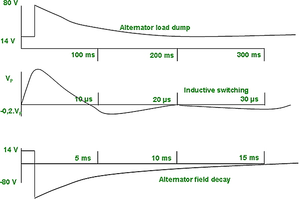
Automotive transients
2.14 Supply voltage phenomenon
The supply voltage can exhibit a variety of disturbances as shown in Figure 2.19.

Supply voltage phenomenon
The ITIC (Information Technology Industries Council) curve shown in Figure 2.20, demonstrates the fluctuation levels and time periods that are likely to upset a PC. From this it is obvious that short-duration voltage variations can definitely affect electronic equipment.
It is just as necessary to ensure that mains-powered equipment doesn’t introduce any of these mentioned phenomena:
- Voltage dips (short-duration reductions in voltage)
- Interruptions (complete absence of power for longer than 3 seconds)
- Harmonics
- Unbalance (voltage differences between phases)
- Flicker (rapid voltage variations which are annoying as they affect incandescent lighting)
- Transients

ITIC Curve
3.1 Introduction
One of the most important aspects in EMC is to understand the difference between the possible modes of coupling. The basis of this differentiation is the idea that two separate circuit paths can coexist in the same set of conductors. The two coupling modes are as mentioned below:
Differential mode – differential simply means the difference between things of the same kind. Differential mode is the normal voltage and current between the signal and its return lines (or for that matter, it can be the positive and negative points in a circuit). Differential (in this case) means the difference between the two lines.
Common mode – common mode comes into the picture when there is another ground (reference) plane with respect to which voltages can exist and currents can flow. Common (here) means common between the two lines and a reference common to them. In common mode the two lines are seen as one.
EMI reduction has a lot to do with solving common mode problems. Common mode paths and voltages are more difficult to understand and visualize in comparison to differential mode. The latter involves current flowing as a normal circuit operation i.e., in loop. However, Common mode does not involve current flowing as per normal circuit operation as it involves multiple coupling paths and parasitic elements.
3.2 DM/CM conversion
Although it is said that common mode currents might be unrelated to the intended signal currents, there may also be a component of common mode current that is due to the signal current. Conversion occurs when the two signal conductors present different impedances to their environment, which is represented by the external ground. These impedances are dominated at RF by stray inductance and capacitance that relate to physical layout and are only under the circuit designer’s control (if and only if that person is also responsible for physical layout).
In Figure 3.1 the differential mode current IDM produces the desired signal voltage across load RL. The common mode current ICM does not flow through load RL directly but through impedances ZA and ZB, and returns back through the external ground. ZA and ZB are not circuit components but distributed stray impedances (typically but not always capacitive) and are determined by factors such as the surface area of PCB tracks and components and their proximity to chassis metalwork and other parts of the equipment. If ZA = ZB then no voltage is developed across RL by the common mode currents ICM. But any inequality (i.e., ZA ≠ ZB) results in such a voltage, proportional to the differences in impedance as given by equation 1:
Vload(CM) = ICM.ZA – ICM.ZB = ICM. (ZA – ZB) …………………..(1)
For this reason, circuits that carry high-frequency signals (such as wideband data or video) or which could be susceptible to RF are best designed in such a way that the stray impedances of each conductor are balanced as near as possible. Alternatively, a common-mode choke is used that swamps the imbalance of the strays and reduces the magnitude of common mode current ICM. The increasing popularity of wideband data transmission through unscreened cables within and between buildings has sharpened the problem of interference radiated from these cables. The balance of the circuit at either end of the cable, the balance of the cable itself as it passes near to other conducting structures in its environment (vicinity), is a prime factor. This is largely determined by the quality of the cable construction, and has resulted in a cable parameter known as longitudinal conversion loss (LCL). The LCL of a balanced cable system is a measure of the mode conversion shown by the system, i.e. the degree to which an inadequately balanced termination and unwanted differential signal will develop when excited by a common mode signal.
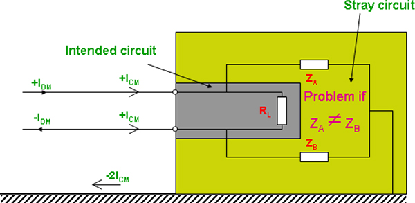
DM/CM conversion
3.3 Common mode rejection ratio (CMRR)
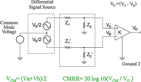
CMRR
CMRR is a measure of how well a system can see the differential signal in the presence of common mode (CM) noise. Figure 3.2 shows such an arrangement to measure CMRR. In this case, the common mode voltage is applied to both the positive as well as the negative terminal of Opamp (Operational Amplifier), while differential mode voltage is applied separately to the positive and negative terminals of the Opamp. K is the gain provided by the Opamp. The voltage at the output of the Opamp due to a common mode signal is the average of voltages VA and VB. Therefore, it can be said that the output due to a common mode signal depends on the individual signal levels at point A and B. On the other hand, voltage at the output of an Opamp due to a differential mode signal is the difference between the voltages VA and VB. Therefore, it can be said that the output due to a differential mode signal does not depend on the individual signal levels at point A and B. CMRR can be represented by the equation 2 given below:
CMRR = 20log10(VCM/Vo) …………………..(2)
where, VCM = (VA +VB)/2 and
Vo = VA – VB
3.4 Units in EMC engineering
There is a wide range of units used right from DC (i.e., 0 Hz) to GHz using logarithmic scales for frequency and μA to kA, μV to MV, etc using decibels (dB) for magnitude. Decibel as a ratio is used to describe relative levels and relative power. A relative base unit such as 1 μV/m is used while describing levels.
X dBμV/m = 20log10(X μV/m / 1 μV/m) …………………..(3)
Examples of Decibel as a ratio are as follows:
0.1 μV/m = –20 dBμV/m
1 μV/m = 0 dBμV/m
3 μV/m = 10 dBμV/m
10 μV/m = 20 dBμV/m
100 μV/m = 40 dBμV/m
3.4.1 The decibel: power
Figure 3.3 shows Vin as the input voltage (Pin = corresponding input power) and Vout as the output voltage (Pout = corresponding output power). 0 dB gain means unity gain as shown in the Figure 3.3. It means that the input power is the same as the output power. Similarly, 3 dB gain doubles the power while, –3 dB gain halves the power and therefore 3 dB points are called half power point.
Power ratio and voltage ratio are given by the equations 4 and 5 respectively:
Power ratio = 10log10(Pout/Pin) …………………..(4)
Voltage ratio = 20log10(Vout/Vin) …………………..(5)

Power ratio and voltage ratio
3.4.2 The decibel: signal to noise (S/N) ratio
‘Signal to noise ratio’, the name itself is self-explanatory; it means the ratio of signal level to the noise level. As shown in Figure 3.4, the signal level at the input is 5 V while the noise level is 0.05 V; therefore the output signal level is 5.05 V i.e., the sum of input signal level and the noise level attached to it. A signal to noise ratio in terms of dB can be represented by equation 6:
S/N = 20log10(Vin/Vnoise) …………………..(6)
From, the example taken in Figure 3.4,
S/N = 20log10(5/0.05) = 20log10(100) = 40dB
The ratio should be as high as possible, i.e., ideally it should tend to infinity.
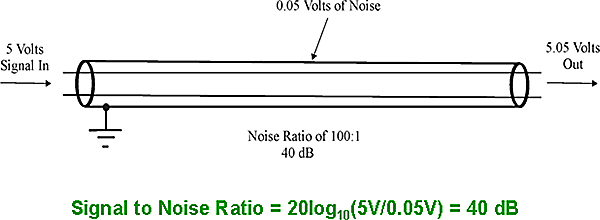
Signal to noise ratio
3.4.3 dBm
One of the most common units expressed in decibels is dB(mW) or dB relative to 1 milliwatt. This is almost always written in the abbreviated form, dBm (i.e. without the “W” and without the parentheses). Many oscilloscopes and spectrum analyzers optionally display voltage amplitudes in dBm. Since dBm is a unit of power, we must know the impedance of the measurement in order to convert dBm to volts. For example, a voltage expressed as 0 dBm on a 50-ohm spectrum analyzer is,
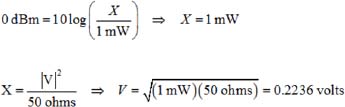
Example 1-3: Specifying voltages in dBm
Specify the following voltages in dBm assuming they were measured with a 50-ohm oscilloscope:

3.5 Spectrum usage and created Interference
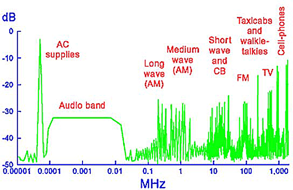
Spectrum usage
Figure 3.5 shows the Electromagnetic spectrum that currently exists ranging from almost 0 Hz (i.e., DC) to around 1 GHz and includes AC supplies, AM, FM, cell-phones, etc. Any equipment required to stay immune should not cause interference within the same band of frequency or other bands of frequencies.
In reality, it is seen that virtually all electronic equipments potentially cause interference in almost all those areas where it is not acceptable. From an EMC point of view it is essential to know exactly where in the frequency spectrum a culprit exists i.e., causes interference and at what frequencies a victim is sensitive i.e., affected by interference caused by others or by itself. Figure 3.6 shows the operating frequencies of an AC supply, switch-mode power supplies and a microprocessor clock along with their harmonics. Due to 50/60 Hz rectifiers, thyristor switches, load switching etc., utility grid interference usually occurs in the Hz to kHz region. On the other hand, switch-mode power supplies operate/switch in the kHz region with harmonics extending into the MHz region.
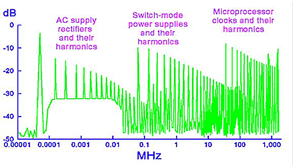
Created interference
3.6 Fourier analysis
Fourier analysis is used to switch between a time domain and a frequency domain. An oscilloscope is used for observing (or viewing) the signals in the time domain, similarly a spectrum analyzer is used for observing (or viewing) the signals in a frequency domain. If a sine wave of time period T is seen on the oscilloscope screen in the time domain, then the corresponding view in the frequency domain on a spectrum analyzer will be a single line as shown in Figure 3.7. The frequency at which this single line will appear on a spectrum analyzer will be Fo, where Fo = 1/T.
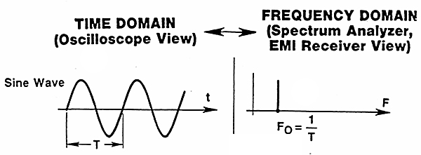
Fourier analysis
3.6.1 Frequency Spectrum of a Pulse

Frequency spectrum of a single pulse
Figure 3.8 shows the frequency spectrum of a single pulse. A single pulse consists of a spectrum of frequencies. There are no distinct frequency components, but rather a smudge of components of variable amplitude. The critical parameter is F2, the effective bandwidth of the pulse; after F2 the spectrum decays quickly.
Figure 3.9 shows the frequency spectrum of a pulsed periodic signal. A pulsed periodic signal consists of a spectrum of discrete frequencies. The critical parameter is F2 as it is the effective bandwidth of the signal. After F2 the spectrum decays quickly.

Frequency spectrum of a pulsed periodic signal
3.7 Choice of logic family
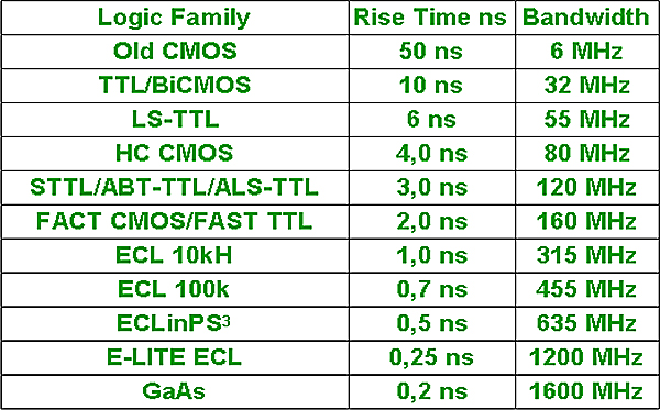
Choice of logic family
The table shown in Figure 3.10 shows the logic family along with the corresponding rise time and bandwidth. The bandwidths for different logic families are calculated using the 1/(πtr) formula. It shows that fast logic can generate a very large noise spectrum.
The damage (as far as emissions are concerned) is done by switching edges having fast rise times (note that this is not the same as propagation delay and is hardly specified in data sheets; where it is a maximum figure). Using the slowest risetime compatible with reliable operation minimizes the amplitude of the higher order harmonics where radiation is more efficient.
The advice is to use the slowest logic family that will do the job; don’t use the fast logic family. Where parts of the circuit operate at high speed, use fast logic only for those parts and keep the clock signals local. This preference for slow logic is unfortunately against the demands of software engineers (of greater processing speeds).
3.8 Lightning and ESD bandwidth
Although lightning and ESD are both pulsed noise, they differ in their treatment and threats. The following are the points that make them two distinct threats:
- The first and foremost is their different bandwidths, lightning is primarily a conductive immunity concern and ESD a radiated immunity concern.
- Lightning is typically a microsecond event; on the other hand, ESD is a nanosecond event.
- The typical bandwidth for lightning is around 300 kHz while that for ESD is around 300 MHz.
4.1 Introduction
Shielding and filtering are two complementary practices. There is hardly any point applying good filtering and circuit design practices to guard against conducted coupling if there is no return path for the filtered currents to take. The shield provides such a return, and also guards against direct field coupling with internal circuits and conductors. Shielding involves placing a conductive surface around the critical parts of the circuit so that the electromagnetic field that couples to it is attenuated by a combination of reflection and absorption. Enclosures, cables, circuits and PCBs are the parts that are to be shielded. The shield can be an all-metal enclosure; if protection will be enough then a thin conductive coating deposited on plastic is sufficient.
The question arises – Why do we shield? The two reasons for shielding are as follows:
- To protect the victims (such as sensitive circuits) from radiated emissions. In many cases victims can be humans (biological hazards). There is an on-going debate on the damage to humans by RF fields. Figure 4.1 shows the chart that gives some guidance on exposure levels for different frequencies.
- To reduce interference from culprits (such as noisy circuits, transmitters).
Shielding is often an expensive and difficult-to-implement design decision, because many other factors (such as tooling, aesthetic, accessibility) work against it. Shielding on a PCB/circuit level does not cost much but shielding on a larger level is usually expensive compared to changing a PCB or even adding a few filters in the design stage. The figures mentioned below shows how shielding of large enclosures adds exorbitant costs. It shows the part that is shielded along with the shielding cost in US dollars.
- Individual IC – US$ 0.3
- Segment of PCB – US$ 1.00
- Whole PCB – US$ 10.00
- Sub-assembly – US$ 20.00
- Whole product – US$ 100.00
- System – US$ 1000.00
- Room – US$ 10000.00
- Building – US$ 100000.00
A decision on whether or not to shield should be taken as early as possible in the project. Interference coupling is via interface cables and direct induction to/from the PCB. You should be able to calculate to a rough order of magnitude the fields generated by the PCB tracks and compare these to the desired emission limit. If the limit is exceeded at this point and the PCB layout cannot be improved, then shielding is essential. Shielding itself does not affect common mode cable coupling and so if this is expected to be the dominant coupling path a full shield may not be necessary. It does establish a clean reference for decoupling common mode currents too, but it is also possible to do this with a large area ground plate if the layout is planned carefully.
Safety precautions
A description of shielding issues can be best classified into two parts:
- The theory of electromagnetic (EM) attenuation through a conducting barrier of infinite range, and
- The degradation of theoretically achievable shielding effectiveness by practical forms of shield construction
4.2 Shielding and Murphy’s Law
From the above section, it is clear that shielding costs much more with size. It is important to make the product cost effective, which suggests – avoid shielding if possible. If the layout allows concentrated interface, a ground plate may be adequate with partial shielding. Design for the possibility of shielding being required with a variety of shields in mind i.e., with many options of shielding in hand.
Murphy’s Law mentions that the shields should have thickness greater than 0.5 mm and should be rectangular in shape. Shields should be as large as possible (the design permitting), and use different, irrational side lengths.
4.2.1 Skin effect and skin depth
The important characteristic of the barrier material is its skin depth δ. This is the distance into the material at which the current density has reduced to 1/e (0.37 or 8.7 dB) due to skin effect. For every distance δ into the material the current density drops by 8.7 dB (approx. 9 dB). The thicker the wall, the greater is the attenuation of the current through it. This absorption loss depends on the number of skin depths through the wall. The skin depth is an expression of the electromagnetic property that tends to confine AC current flow to the surface of a conductor, becoming less as frequency, conductivity or permeability increases.
Skin depth (δ) = (π.F.μ.σ)-0.5 meters
where, F = frequency,
σ = conductivity,
μ = permeability
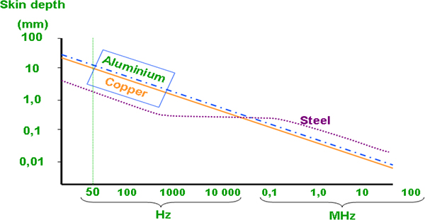
Skin depth for copper, aluminium and steel
Figure 4.2 shows the skin depths of copper, aluminium and steel. For example, skin depth in aluminium at 30 MHz is 0.015 mm. This explains why thin conductive coatings are effective at high frequencies – the current flows only on the surface, and the bulk of the material does not affect the shielding properties. It is therefore possible to reduce the current density by 18 dB in material with twice the thickness (i.e., with two skin depths), and 27 dB if it’s thrice the thickness (i.e., with three skin depths), and so on. The requirements for an effective shield are high conductivity for electric fields and high permeability for magnetic fields.
4.2.2 Shielding principles

Applying the concepts of shielding effectively requires an understanding of the source of the interference, the environment surrounding the source, and the distance between the source and point of observation (the receiver). If the circuit is operating close to the source (in the near, or induction-field), then the field characteristics are determined by the source. A circuit operates in a near-field if its distance from the source of the interference is less than the wavelength (λ) of the interference divided by 2π, or λ/2π. If the circuit is remotely located (in the far, or radiation-field), then the field characteristics are determined by the transmission medium. If the distance between the circuit and the source of the interference is larger than this quantity, then the circuit operates in the far field.
For instance, the interference caused by a 1-ns pulse edge has an upper bandwidth of approximately 350 MHz. The wavelength of a 350-MHz signal is approximately 857 mm (the speed of light is approximately 300mm/ns). Dividing the wavelength by 2π yields a distance of approximately 5 inches, the boundary between near- and far-field. If a circuit is within 127mm of a 350-MHz interference source, then the circuit operates in the near-field of the interference. If the distance is greater than 127mm, the circuit operates in the far-field of the interference.
Regardless of the type of interference, there is a characteristic impedance associated with it. The characteristic, or wave impedance of a field is determined by the ratio of its electric (or E-) field to its magnetic (or H-) field. In the far field, the ratio of the electric field to the magnetic field is the characteristic (wave impedance) of free space, given by Zo = 377 Ω. In the near field, the wave-impedance is determined by the nature of the interference and its distance from the source. If the interference source is high-current and low-voltage (for example, a loop antenna or a power-line transformer), the field is predominately magnetic and exhibits a wave impedance which is less than 377 Ω. If the source is low-current and high-voltage (for example, a rod antenna or a high-speed digital switching circuit), then the field is predominately electric and exhibits a wave impedance which is greater than 377 Ω.
Conductive enclosures can be used to shield sensitive circuits from the effects of these external fields. These materials present an impedance mismatch to the incident interference, because the impedance of the shield is lower than the wave impedance of the incident field. The effectiveness of the conductive shield depends on two things: First is the loss due to the reflection of the incident wave off the shielding material. Second is the loss due to the absorption of the transmitted wave within the shielding material. The amount of reflection loss depends upon the type of interference and its wave impedance. The amount of absorption loss, however, is independent of the type of interference. It is the same for near- and far-field radiation, as well as for electric or magnetic fields.
Reflection loss for plane waves in the far field decreases with increasing frequency because the shield impedance, Zs, increases with frequency. Absorption loss, on the other hand, increases with frequency because skin depth decreases. For electric fields and plane waves, the primary shielding mechanism is reflection loss, and at high frequencies, the mechanism is absorption loss.
Thus for high-frequency interference signals, lightweight, easily worked high conductivity materials such as copper or aluminum can provide adequate shielding. At low frequencies however, both reflection and absorption loss to magnetic fields is low. It is thus very difficult to shield circuits from low-frequency magnetic fields. In these applications, high-permeability materials that exhibit low-reluctance provide the best protection. These low-reluctance materials provide a magnetic shunt path that diverts the magnetic field away from the protected circuit. Examples of high-permeability materials are steel and mu-metal.
To summarize the characteristics of metallic materials commonly used for shielded purposes: Use high conductivity metals for HF interference, and high permeability metals for LF interference.
The frequency of the interfering signal is a critical concern when selecting EMI shielding devices. Low frequency magnetic waves in the 1 to 30 KHz range, for example, are most effectively shielded by absorbing the signals in permeable material. High frequency signals (30 KHz and above) are most effectively shielded by reducing entry windows and by insuring adequate surface conductivity to ground.
A properly shielded enclosure is very effective at preventing external interference from disrupting its contents as well as confining any internally-generated interference. However, in the real world, openings in the shield are often required to accommodate adjustment knobs, switches, connectors, or to provide ventilation. Unfortunately, these openings may compromise shielding effectiveness by providing paths for high-frequency interference to enter the instrument. The longest dimension (not the total area) of an opening is used to evaluate the ability of external fields to enter the enclosure, because the openings behave as slot antennas. Equation below can be used to calculate the shielding effectiveness, or the susceptibility to EMI leakage or penetration, of an opening in an enclosure:

where λ = wavelength of the interference and L = maximum dimension of the opening Maximum radiation of EMI through an opening occurs when the longest dimension of the opening is equal to one half-wavelength of the interference frequency (0-dB shielding effectiveness). A rule-of-thumb is to keep the longest dimension less than 1/20 wavelength of the interference signal, as this provides 20-dB shielding effectiveness.
Furthermore, a few small openings on each side of an enclosure is preferred over many openings on one side. This is because the openings on different sides radiate energy in different directions, and as a result, shielding effectiveness is not compromised. If openings and seams cannot be avoided, then conductive gaskets, screens, and paints alone or in combination should be used judiciously to limit the longest dimension of any opening to less than 1/20 wavelength. Any cables, wires, connectors, indicators, or control shafts penetrating the enclosure should have circumferential metallic shields physically bonded to the enclosure at the point of entry. In those applications where unshielded cables/wires are used, then filters are recommended at the shield entry point.
LF magnetic shielding
Shielding against magnetic fields at low frequencies is to all intents and purposes impossible with purely conductive materials. This is because the reflection loss to an impinging magnetic field (RH) depends on the mismatch of the field impedance to the barrier impedance. The low field impedance is well matched to the low barrier impedance and the field is transmitted through the barrier with only a few dB attenuation or absorption. Fortunately, the requirements of the EMC Directive generally don’t extend to magnetic shielding at low frequencies, with the possible exception of some types of apparatus that may be susceptible to power frequency fields.
A high-permeability material such as mu-metal or its derivatives can give LF magnetic shielding by concentrating the field within the bulk of the material, but this is a different mechanism to that discussed above, and it is normally only viable for sensitive individual components such as CRTs or transformers. For an infinitely long cylinder in a DC field the shielding factor is:
SM = μ/2 × t/d
where, μ = material permeability,
t/d = ratio of material thickness to cylinder diameter
Practically, there is a fall off of shielding performance towards the ends, but for distances inside the cylinder greater than the diameter the shield can be regarded as infinitely long; alternatively a high-permeability end cap can be used. Both welded seams and high intensity fields have the effect of reducing the material permeability μ. High flux densities tend to saturate the material; if this is likely then increase the material thickness or use a double shield with a nested construction, with a higher saturation flux density material facing the impinging field. For prototyping, you can use foil magnetic shielding material that can easily be worked by hand. Production shields should be properly fabricated and this needs to be done by a specialist.
4.3 Apertures and shielding effectiveness
Shielding effectiveness vs frequency
The graph shown in Figure 4.3 shows how shielding effectiveness (SE) deteriorates with frequency and aperture dimension. A 100 mm aperture will roughly let through 20 dB more than a 10 mm one. Apertures are needed for ventilation, control and interface access, and for viewing an indicator. Seams, i.e., discontinuities at the joints between individual conductive members, also act as apertures.
Much academic effort has been spent in trying to quantify the general effect of apertures and discontinuities in shielding. Apart from the special case of sphere, a simple analytical expression based on the fundamental field equations has been unobtainable, leaving us until recently with recourse either to numerical computer modeling of a particular situation, or to various empirical rules of thumb. The possible number of variables that compound the difficulties are as mentioned below:
- The shape, size, position and number of apertures
- The relative positions and distances between the field source, the shield barrier and the apertures in it, and the victim
- The geometry of the shielding enclosure
- The frequency and source impedance of the field
All of these have to be taken into account by the model, even when considering the possible variations in the properties of the shielding material itself.
If adequate computing resources and skilled modeling staff are available, some shielding problems can be successfully modeled by numerical methods and substantial academic work has gone into improving these. Results have yet to be made available in a useable form to wider industry applications. This leaves us with some general guidelines and a few simplistic equations. The most widely quoted of these equations is
SE = 20 log (λ/2l) dB (below resonance)
where, λ = wavelength,
l = maximum aperture dimension
The above equation suggests that the shielding effectiveness (SE) degrades proportionally to frequency and is inversely proportional to aperture size until the aperture size is a half wavelength, at which point shielding is zero. This highlights the general dependence on frequency and size of aperture; i.e., the larger the aperture, the greater is its effect and the higher the frequency, the less is the available shielding. But as a means of predicting actual shielding effectiveness the equation is quite inaccurate, since SE also depends on the dimensions of the enclosure and the point at which SE is measured.
The lambda by twenty (λ/20) is a good rule of thumb for establishing maximum aperture size. For aperture(s) with the longest dimension of λ/20, the shielding effectiveness (SE) will reduce by 20 dB. Considering this situation, the distance between fastening screws, apertures, holes, etc. should be less than λ/20.
4.4 Waveguides
If necessary, improved shielding of vents can be obtained at the expense of thickness and weight by using honeycomb panels, in which the honeycomb pattern functions as a waveguide below cut-off. Figure 4.4 shows the dimensions of a waveguide. Figure 4.5 shows the graph of Shielding Effectiveness (SE) vs Frequency. Waveguides have better shielding effectiveness (below the cut-off frequency) than two-dimensional apertures.

Dimensions of waveguides

Shielding effectiveness vs frequency
4.5 Gasketting and sealing
Closer spacing of fixing points gives better control of higher frequencies and/or higher powers, although if more frequent bonds are required it may be easier to slip a length of a suitable EMC gasket material between the mating surfaces. The main parameters with gaskets are:
- Mechanical compliance
- Corrosion resistance
- Operation rate/day before becoming ineffective
- Environmental sealing, etc.
The pressure of the fixings should be sufficient to squeeze the gasket over the entire distance between the fixings with a pressure in excess of its minimum specification. Where the metalwork is less than sturdy, the pressure of the gasket material may make it bow between the fixing and look untidy. Worse than this, the metal may be bowed so much that a gap is opened up and the purpose of the gasket defeated. Additional strengthening plates may be found necessary to prevent this bowing, or else a lower-pressure gasket material could be used.
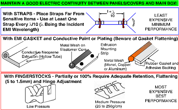
Gasketting and sealing
A very wide variety of gasket materials and products are now available, some of them at low cost, and some with additional chemical or environmental properties. To achieve good contact without excessive pressure, Beryllium-copper or stainless steel spring fingers may be used instead of foam or mesh type gaskets. Care must be taken to ensure that the gasket materials are compatible with the metal types being bonded, taking account of the environment (condensation, spray, corrosive gases, etc.) to ensure that the electrical bonds last the life of the installation.
4.6 Panel displays and keyboards
As shown in Figure 4.7, a dirty box can be constructed to reduce radiation from panel displays. Note that the connections to the display are filtered when going through the clean/dirty box barrier. If a system does not have a clean/dirty box construction, it will typically require a mesh in front of a display to attenuate unwanted radiation. Eg – a Digital Panel Meter as shown in figure below.
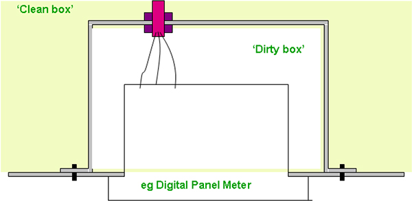
Dirty Box
4.6.1 Shielding displays
Figure 4.8 shows the arrangement for shielding displays. The different layers are as shown below, the wire mesh will let through light but attenuate RF. Note that an EMC gasket must be used to keep radiated noise from creeping around the mesh.

Shielding displays
4.7 Ventilation and shielding
One application for waveguide tubes is to provide ready-made ventilation panels for shielded enclosures. Since the walls of the waveguide can be made quite thin and the tubes can be stacked together with little effect on the electromagnetic attenuation, an assembly of such tubes can be stacked together with little effect on the electromagnetic attenuation. An assembly of such tubes can be built to provide a high degree of through airflow as well as high level of attenuation. These are available as pre-packaged units known as honeycomb panels which can be simply be fitted into the wall of an enclosure to give any reasonable level of the same open area in a thin panel, but of course are more costly and require some thickness in addition to the panel. The wire mesh approach may be adequate for many low-performance applications. To avoid variations in attenuation due to wave polarization, it is common to stack two layers of honeycomb panel against each other, with different orientations of the waveguide tubes in each layer.
4.7.1 Shielding non-metallic enclosures
The conductive coating may be technically feasible. There can be problems at the joints; parts get distorted during tightening. Gasketting is also not very effective. Nickel is effective but there are problems with skin depths/coating thickness. At the same time shielding of electronics should be considered.
Figure 4.9 shows the shielding types/technologies. Conductive coatings can be an alternative to solid metal shields.

Shielding types/technologies
Cables entering and leaving an enclosure should have their screens properly terminated to the enclosure wall. This means that a full 360° contact should be maintained around the outer surface of the cable screen.
Mechanisms for ensuring this are similar to conventional cable glands for environmental sealing, except that the appropriate parts are fully conductive. Most of the traditional manufacturers of cable accessories are now aware of the importance of EMC aspects, and provide EMC-specific cable glands as part of their stock range. A typical construction using tapered washers to compress an iris-type spring against the cable screen outer surface. This is one of the most common methods of clamping to the screen, but others are possible, including collect or other clamping mechanisms, elastometric compression modules, or folding the screening braid back over a conductive tube.
Aspects that you need to consider when specifying a screening cable gland system are:
- Mechanical compatibility – the cable screen outer diameter must match the gland’s construction, often within quite tight tolerances
- Electrochemical compatibility – the materials used for screen, gland and enclosure panels should discourage corrosion
- Ease of assembly, especially if unskilled or poorly trained technicians are expected, or the working area is restricted
- Conductivity across the joints, which directly affects shielding effectiveness
- Least disturbances of the screen
- Whether or not an environmental seal is also required
4.8 PCB-level shielding
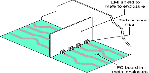
PCB-level shielding
It uses principles similar to shielding modules.
- No holes in the shielding
- Use filters at the interface
- Consider the reference plane as a part of the shield
- Bond the shield to the reference plane at regular intervals
- Consider guarded striplines at entry/exit points (equivalent to screened cables)
Figure 4.11 is an example of shielding on a PCB. Note that there are holes in the shield, but it does not affect shielding effectiveness (SE) if they are small enough.

VHF/UHF shielding on PCB
5.1 Introduction
There has always been confusion between the terminologies Earthing and Grounding. In conventional electrical usage, Grounding is American for the same function as Earthing is in English; i.e., a safety protective function. But the EMC functions are different; the word Grounding will be used to distinguish the EMC function while Earthing will be used for the safety function.
The recognized and accepted purpose for grounding is to give a reference for external connections to the system. The classical definition of a ground is an equipotential point or plane that serves as a reference for a circuit or a system. Unfortunately this definition does not carry any meaning in the presence of ground current flow. Even when signal currents are negligible, induced ground currents due to environmental magnetic or electric fields will cause shifts in ground potential. A good grounding system will reduce these potential differences by comparing the circuit operating levels, but it cannot completely discard them. It has been suggested that the term Ground (as conventionally used) should be replaced with reference point to make the purpose of the node clearer.
An alternative definition for a ground is a low impedance path by which current can return to its source. This emphasizes current flow and the consequent need for currents always circulating as part of a loop. The task here is to design the loop in such a way that induced voltages remain low enough at critical places. Designing the ground circuit to be as compact and as local as possible is the only way to do this. The primary EMC function of a ground system is to minimize interference voltages at critical points compared to the desired signal. For this, it must present a low transfer impedance path at these critical locations.
The major part of the problem has been that different practices are suitable for different purposes; even if the purpose is purely EMC, frequency range is an important parameter, and its relevance is generally misinterpreted.
5.2 Earth and safety ground
Grounds fall in to two main categories:
- Safety ground (also called Earth)
- Signal ground
Signal grounds may or may not be at Earth potential, but safety grounds have to be at Earth potential. One ground should not be used for both signal ground and safety ground.
Figure 5.1 shows how disconnecting earth wires may cause shock hazards. This can happen with a so-called clean ground. A Clean ground can be good from a noise point of view, but unsafe.
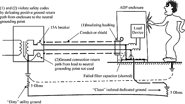
Safety ground causing hazards
Before the IC chip revolution of the ’80s most systems were connected to a common single ground system. This had the advantage of being cheap, efficient and safe. Since all devices were (theoretically) at the same voltage level (0 volts), a person touching two devices would not get ‘shocked’. This system of connecting devices together and then to a single common ground point was abandoned in the late 1980s and 1990s due to excessive noise being transmitted through the common ground into sensitive microcontroller devices. Terms such as clean and digital ground came into use. These grounds were often completely separate from dirty ground systems. It was found in the 1990s that although this system of separate grounds was good from a noise position, it was considered unsafe. This is because by separating the grounds the voltage level of two or more devices would float. This could possibly make devices have difference voltages and therefore render them unsafe.
Figure 5.2 shows a safe setup with the enclosure grounded/ earthed. All device grounds are required to be connected together at one common point. To reduce the noise induced into sensitive IC equipment the quality of the ground must be increased over the simple single point grounding systems of the past. By putting in grid grounds and parallel common point ground the noise induced into devices from other commonly connected grounds can be reduced. Also, since the devices are connected together their ground voltage levels should be at the same level and therefore safe.
With the boost in the use of mobile transmitting devices, EMI safety has taken on a new dimension. Mobile telephones have been known to cause fires at gas stations, turn devices on and cause machinery to act unpredictably. This problem has the potential to cause catastrophic failures in systems, which in turn could cause major accidents, injuries and death.

Safety ground – safe setup
5.2.1 Ground types
One ground does not essentially fit all. Different types of grounds have different current and frequency requirements. Figure 5.3 shows the types of grounds along with their corresponding Bandwidth, Time scale and Level.
| Type | BW | Level | Timescale |
|---|---|---|---|
| Power safety | 50/60 Hz | 10 to 1000 A | Sec to min |
| Lightning | 1 MHz | Upto 100 kA | msec |
| ESD | 300 MHz | 10 to 50 A | nsec |
| EMI | DC to daylight | μA to A | Nsec to years |

Ground types
5.2.2 Objective of Earthing
For instance, any practical structure has non-zero impedance between any two points, and when a current passes through such an impedance a voltage is developed across it. In practice, an EMC engineer is always trying to minimize the interference voltages developed in the earth, and therefore the main requirement for a good earth design is that it should offer minimum impedance to interference currents (whatever it may be) flowing through it. When a circuit is designed to use the earth as its functional return path (by intentionally connecting the returns of the source and load to the earth structure rather than connecting to each other), then the path between these points should have the minimum impedance.
Of the two main considerations for grounds (i.e., current capability and frequency requirements), frequency is the most important for EMC.
5.3 Grounding and frequency
Different types of techniques are used for grounding. Some of them are used at low frequency while others are used at high frequency. These can be classified as follows:
- Low frequency phenomena/technique
- High frequency phenomena/technique
Figure 5.4 shows the range of frequencies by which these techniques are partitioned as low and high frequency techniques. The low frequency techniques ranges from DC (i.e., 0 Hz) to around 10 kHz, while high frequency techniques ranges from 10 MHz to GHz. The crossover region (i.e., between 10 kHz to 10 MHz) of what is considered as high or low frequency grounds can be related to the λ/20 rule. These techniques are a function of frequency, but sometimes they may sound conflicting, e.g., on one hand, single point grounding and on the other hand, planes or grids.

Frequency range
5.3.1 High frequency ground implementation
At high frequencies, there is nothing such as a single point ground because current will flow in return paths through stray/parasitic capacitance and so single point ground will be ineffective. Any conductor in close proximity to an earth/ground structure will have at least a few pF of stray capacitance between them. In the MHz region (and above), even a pF of capacitance will have current flowing through it. At high frequencies, circuits and grounds may not be in contact with each other, but current (i.e., stray/leakage) will flow. If the current to ground is flowing everywhere and anyhow, prevent it and rather make sure it gets dumped to ground through a low impedance path. Use multi-point ground for high frequency ground implementation.
At low frequencies (i.e., below 10 kHz region), star ground topology proves to be the best. Ground loops and common mode impedance coupling generally affect low frequency ground implementation.
5.4 Ground loops
Modern day industries and businesses rely largely on electronic systems. These include industrial drives, distributed control systems, computer systems and networking equipment or communication electronics. These electronic devices often work with very low power and voltage levels for their control and communications and cannot tolerate even small over voltages or currents. The result of such voltage/power surges is invariably the failure of the electronic device itself. It is also possible that induced voltages from nearby power circuits experiencing harmonic current flow can cause interference in the systems carrying communication signals and can result in malfunctions due to erroneous signal transmission. Due to this sensitive nature of electronic and communication equipment, any facility that houses such equipment needs to have its electrical wiring and grounding systems planned with utmost care so that there are no unpredictable equipment failures or malfunction.
One of the important and main factors of concern is the noise due to Ground loops. Figure 5.5 shows the illustration of how a ground loop is formed between the grounds of two circuits (circuit 1 and circuit 2).

Ground loop illustration
Ground loops are problems because currents return in the ground circuit by separate paths. Separate paths have different impedances and cause ground voltages that shift with respect to each other. This shifting of the grounds is seen as noise in the circuitry, and therefore a practice has been developed of trying to discard all such loops. This practice may although often be superficially successful but is unfortunately misguided.
Consider a situation where high earth potential differences exist, and closing a loop between two such earth points will allow a high current to flow in the structure. If the conductors in that loop include a segment that either forms part of, or is closely coupled to a signal or low-level power cable, then substantial interference will be induced in that cable. If the loop is not closed (i.e., opened), the current no longer flows, and hence no interference – although the high potential differences still remain and is ready to create interference as soon as another loop is formed somewhere else. This is the principle that is now a convention in the star or single point earth regime – remove all ground loops and live with the resultant high voltages between different parts of the earthing system.
In low frequency systems, such an approach is fairly easy to implement and at the same time is also quite successful, but it represents a retreat from best practice. Now that interference is typically measured in the MHz region rather than Hz, it is untenable. This is because earthing conductors provide high impedance at these frequencies and therefore they tend to de-couple a system from earth, rather than couple to it. Another effect of ground loops is that they act as magnetic/inductive loops (or antenna). Magnetic flux couples through the loop and induces a noise voltage that shifts the ground.
In these circumstances the only reliable and efficient earthing system is a mesh. The mesh provides a multiplicity of ground loops (but they are small and controlled) – potential differences between parts of the structure are reduced, resulting currents are low and the interference consequences (if any) are negligible. The safety, reliability, ease of use and EMC advantages of properly implemented MESH-BN systems by far outweighs their possible disadvantages.
5.5 Ground impedance
Earthing wires do not offer end-to-end low impedance at high frequencies. Even at moderate frequencies, their impedance is quite significant. Ground impedance depends on the frequency:
- At DC (and low frequency) the impedance is purely resistive.
- In the medium frequency range, the impedance is inductive. The impedance of the length of wire increases linearly with frequency as long as the inductance dominates.
- At higher frequencies, transmission line and antenna effects are evident.
A piece of wire is not a high frequency connection, use bonding straps instead as it works because of its large area. At high frequency, current crowds towards the surface of the conductor (skin effect), for this current to have low impedance, it must flow freely across the large area.
5.6 Ground topologies
Grounding systems for a circuit reference can be configured by either of the below mentioned three ways:
Single point ground – the single point grounding system is conceptually the simplest, and it reduces common impedance ground coupling and low frequency loops. Figure 5.6 shows the single-point ground configuration.
Each rack or sub-unit has one bond to the chassis, and each circuit module has its own connection to a single ground. Any currents flowing in the rest of the ground network do not couple into the circuit. Such a system works well up to frequencies in the MHz region, but the distances involved in each ground connection means that the common mode potentials between circuits start to build up as the frequency increases. The circuits are effectively isolated from each other at distances of odd multiples of a quarter wavelength and at the same time, stray capacitance starts to contribute to sneak current- paths that bypass the single point wiring.
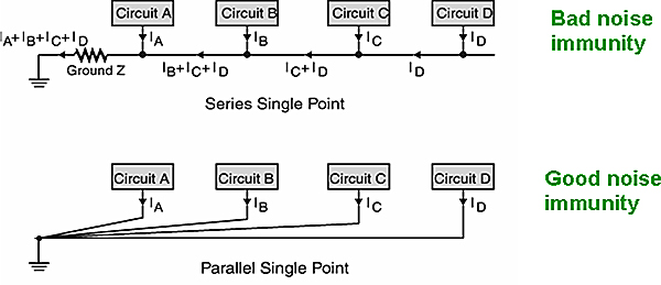
Single-point ground
Multi-point grounding – Figure 5.7 shows the multi-point ground configuration.

Multi-point ground
Multi-point grounding and hybrids can overcome the RF problems associated with the pure single-point systems. Multi-point grounding is mandatory for digital and large signal high-frequency systems. Circuits and modules are bonded together with many short links to reduce ground-impedance-induced common mode voltages. Alternatively, many short links to a chassis, ground plane or other low impedance conductive body are made. If the loops are formed then they may cause magnetic field pick-up, and hence this may not be suitable for sensitive audio circuits. It is difficult to keep the supply frequency (50/60 Hz) interference out of such circuits. But this is only a problem if the circuits themselves are prone to it and if amplitudes are large because the loop areas are large. Circuits that operate at high frequencies are not susceptible to this interference.
Hybrid grounding – In hybrid grounding systems, reactive components such as capacitors and/or inductors are used to make the grounding system act differently at low frequencies and at RF (high frequencies). With a hybrid ground a capacitor is used to complete the ground circuit. At low frequencies where ground loops are the problem, the capacitor will tend to isolate the grounds. At high frequencies, capacitors act as shorts and multi-point grounds result.
5.7 Guidelines for grounding
It is not practical to optimize the ground layout for all individual signal circuits, so circuits with the greatest threats should be concentrated on. These are the ones that most frequently carry the high di/dt signals (clock lines and data lines, and square wave oscillators at high powers, especially in switching power supplies). From a susceptibility point of view, sensitive circuits (such as edge-triggered inputs, clocked systems, and precision analog amplifiers) should be treated similarly. After identification and partition of these circuits, loop inductance and ground coupling are concentrated. Here are the guidelines made for grounding:
- Don’t compromise on safety grounds
- Analog circuit grounds
- Digital circuit grounds
- I/O grounds
- Ground Map
5.7.1 Grounding analog circuits
The prime objective here is to prevent noisy ground currents to interfere with sensitive analog ground paths. Analog circuits such as motors, relays etc. fall in the low frequency region and should be grounded by single star point. Extra measures, such as separate or filtered power and local grounds, should be taken depending on circuit sensitivity. Separate analog, digital and power grounds should be present and they can be joined at a single point generally at an A/D or D/A converter. If there are more than one A/D or D/A converters, use more than one ground plane (Figure 5.8).

Multiple analog circuits
5.7.2 Grounding digital circuits
The prime objective here is to obtain lowest ground-path impedance. Because of the fast rise time and fall time, digital return currents are also of high frequency and so use high frequency multi-point grounds and ground planes. If the circuit is placed in a metal enclosure, then provide multiple high frequency grounds to the chassis (i.e., capacitors) as it lowers the board-to-board and board-to-chassis resonance.
5.7.3 I/O grounding
The prime objective here is to prevent the circuits from becoming unintended transmitters and receivers and to prevent the cables from becoming unintended antenna. Figure 5.9 shows that a digital ground plane should never be extended over an analog section, as this will couple digital noise in analog circuitry.

I/O Grounding illustration
A single point connection between analog and digital grounds can be made at the systems A/D (Analog to Digital) converter. It is very important here to not connect the digital circuitry separately to an external ground, and if this is done then extra current paths are set up that permit digital circuit noise to circulate in the clean ground. Interfaces to the digital circuits (for instance, an input or output port) should be buffered so that there is no need to be referenced to the digital 0 V. The best interfaces available are an opto-isolator or relay, but these are expensive. When isolation cannot be afforded, a separate buffer IC that can be referenced to the I/O ground is preferable, otherwise buffer the port with series resistors or chokes and decouple the line at the board interface with a capacitor and/or a transient suppressor to the clean ground.
5.7.4 The ground map
The objective here is to avoid and control grounding-problems in the design stages itself and also plan grounds at the same level. A fundamental tool for use throughout the equipment design is a ground map. This is a diagram that shows all the ground reference paths and grounding paths (via structures, cable screens etc. as well as tracks and wiring) for the whole equipment. It concentrates on grounding only; all other circuit functions are omitted or shown in block form. Its creation, maintenance and enforcement throughout the project design should be the responsibility of the EMC design authority.
The technique used is as follows:
- Identify all the grounds i.e., safety, analog, digital, module, etc.
- Construct ground map i.e., ground diagram.
- Analyze and correct ground paths, common impedance coupling, sneak paths, etc.
5.7.5 Selection of a Grounding Scheme
The facts are that a single-point grounding scheme operates better at low frequencies, and a multipoint ground behaves best at high frequencies. If the overall system, for example, is a network of audio equipment, with many low-level sensors and control circuits behaving as broadband transient noise sources, then the high-frequency performance is irrelevant, since no receptor responds above audio frequency. For this situation, a single-point ground would be effective. Conversely, if the overall system were a receiver complex of 30 to 1,000 MHz tuners, amplifiers, and displays, then low-level, low-frequency performance is irrelevant. Here, multipoint grounding applies, and interconnecting coaxial cables should be used.
The above comparison of audio versus VHF/UHF systems makes clear the selection of the correct approach. The problem then narrows down to one of defining where low- and high-frequency crossover exists for any given subsystem or equipment. The answer here in part involves the highest significant operating frequency of low-level circuits relative to the physical distance between the farthest located equipments. The determination of the crossover frequency region involves consideration of (1) magnetic versus electric field coupling problems and (2) ground-plane impedance problems due to separation. Hybrid single and multipoint grounding systems are often the best approach for crossover region applications.
When printed circuits and ICs are used, network proximity is considerably closer. Thus, multipoint grounding is more economical and practical to produce per card, wafer, or chip. Interconnection of these components through wafer risers, motherboards, etc. should use a grounding scheme following the illustrations of previous paragraphs. This will likely still represent a multipoint or hybrid grounding
approach in which any single-point grounding (for hybrid grounds), if used, would be to avoid low-frequency ground current loops and/or common- mode impedance coupling.
In summary, many system-level EMI problems can be avoided by paying careful attention to the grounding scheme used. Common-mode, common-ground impedance problems may be reduced by application of one or more of the following techniques.
• Eliminate common impedance by using a single point ground (Fig. 5.6) if possible. This configuration is usually optimal for power frequencies and signal frequencies below 300 kHz.
• Separate and isolate grounds on the basis of signal type, level, and frequency as illustrated in Fig. 5.10.
6.1 Introduction
Cabling between equipments is a principal route for interference coupling, both into and out of equipments. Due to their length these are more efficient at interacting with the electromagnetic environment than enclosures, PCBs or other mechanical structures. Cables themselves are passive, and therefore do not come within the scope of any EMC regulations. Although there are occasional sales claims, to the effect that, certain cable types comply with the EMC Directive or FCC rules, such claims are not genuine. However, use of a particular type of cable may enable a system or apparatus to comply with EMC requirements. Choice of cables and connectors is a crucial aspect of system design for EMC. Cables and connectors that form the interface to the equipment must be carefully specified. The main purpose of this is, to ensure that, differential mode signals are prevented from radiating from the cables, and the common mode cable currents are neither impressed on the cable by the signal circuit nor are coupled into the signal circuit from external fields via the cable.
Layout, routing and terminations will all affect coupling of interference to or from the cables and can therefore have an impact on the overall system performance. The equipment designer needs to specify a particular cable type for a particular interface in order to meet EMC requirements for the equipment; the system designer will have to ensure that this is used, and needs to implement the best installation practice.
In many cases, screened cables are used. The usual exceptions are the mains power cable (provided a mains filter is connected), and low-frequency interfaces that can be properly filtered to provide transient and RF immunity. An unfiltered, unscreened interface will provide a path for external emissions and for undesired inward coupling. The way that the cable screen is terminated at the connector interface is critical in maintaining the screening properties of the cable.
6.2 Cables in context
The function of a cable is to convey a signal or power from one point to another. For this, the type and size of conductor is important. Usually power transmission is done at low frequency. High frequency signals require twisted pair, co-axial cables or waveguides.
A crucial initial stage in the EMC control of any system is to assess the electromagnetic environment that will be enjoyed (for that matter, suffered) by the system. This will in turn, define the degree of severity, that will be needed by the system’s components in dealing with various phenomena, in the levels of stimulus or limits of emissions that are applied, and in the amount of degradation of functional performance, allowed for each function, for each disturbing phenomenon. The various product and generic standards that are available, to some extent, present such a picture of the environment, but only in broad terms. For a closer match, for any given system, a more specific review of the intended environment is required. While designing a product to a specification without knowledge of the system or environment in which it will be installed, there exists two aspects viz., emissions and susceptibility, and the product has to be designed to meet the minimum requirements for each. Limits are laid down in various standards, but individual customers or market sectors may have more specific requirements. In those standards that derive from CISPR (International Special Committee for Radio Interference), emissions are subdivided into radiated emissions from the system as a whole, and conducted emissions present on the interface and power cables. Conventionally, the breakpoint between radiated (high frequency) and conducted (low frequency), is set at 30MHz (primarily for convenience of measurement). Radiated emissions can themselves be separated into emissions that derive from differential currents on internal PCBs or other wiring, and emissions from common-mode currents on PCBs or conducting structures, or that find their way onto external cables that are connected to the equipment.
Electronic equipment will be susceptible to environmental electromagnetic fields and/or to disturbances coupled into its ports via connected cables. An Electrostatic discharge may be coupled in, via the cables or the equipment. A nearby discharge can also create a local field that couples directly with the equipment. The potential threats are as mentioned below:
- Electrostatic discharge (ESD)
- Radiated RF fields
- Magnetic fields
- Conducted transients
- Supply voltage disturbances
Apart from the legal requirements, equipment that is designed to be immune to these effects (especially ESD and transients) will save its manufacturer’s expense considerably, through improved reliability and reduced field returns. Although many aspects of emission control are also relevant for immunity, in some cases the shielding and circuit suppression measures that are required for protection against ESD or RF interference may be more than needed, for simple compliance with emission standards.
From the EMC point of view, a cable can either cause emission or receive emission, as described above as emission and susceptibility. This will depend on the type of cable as well as the screening and grounding arrangements.
6.3 Cable parameters and implication
Any current carrying conductor can produce an Electromagnetic (EM) field. The inverse of this is also true i.e., any conductor can convert electromagnetic fields into current. The conductor longer than λ/20 will start acting as an Antenna. λ is the wavelength of the highest frequency of concern and is given by the equation,
λ = c/f
where f = frequency in Hz
c = 3 × 10⁸ m/s, speed of light
All the cables are not the same in functioning and therefore a correct cable should be selected for the job. Here are some of the points that show, how overlooking cable parameters can produce unexpected effects.
- 1 meter wire is equivalent to an inductor of 1μH, where resistance is greater than 6 Ω at 1 MHz.
- Resistance of a wire of diameter 1 mm at 160 MHz is equivalent to 50 times its resistance at DC (0 Hz).
- 25 mm long wire of radius 1mm is equivalent to a capacitor of 1pF.
- 100 mm earth wire is equivalent to an inductor of 100 nH, where filter effectiveness is equal to zero at frequency greater than 5 MHz.
6.4 Cable types and frequency

Classification of cables
To minimize crosstalk effects within a cable, the signals carried by that cable should all be approximately equal in current and voltage. This leads to the grouping of cable classifications as shown in Figure 6.1. Cables carrying high frequency interfering currents should be kept away from other cables, even within shielded enclosures, as the interference can readily couple to others nearby and generate conducted common mode emissions. As shown in Figure 6.1, cables can be classified as follows:
- Noisy
- Slightly noisy
- Slightly sensitive
- Sensitive
Normal wire pairs are used for power applications or signals up to a few Hz. From a few hundred Hz to kHz, wires should be twisted i.e., twisted pair should be used. Shielded twisted pairs work well for signals up to a few hundred kHz. In the MHz range, cables start showing transmission line effects, and so the cables should be either co-axial cables or high quality twisted paired. In the GHz range, co-axial cables become ineffective and therefore waveguides are used.
It is very difficult to agree on certain points – for relatively short connections (around 100 m), opt for non-conducting media. After trying this method out for a few days, to sort out the source of EMC problems using conductors, the only solution left is to go for non-conducting media such as:
- Microwave or LASER links
- Fibre optic links
- Infra-red
- Wireless Ethernet or TETRA or Blue-tooth
The above-mentioned non-conducting mediums are opted in comparison to conducting cables because conductors tend to leak and/or attenuate the signal or power. Intended differential currents are partially converted to common mode currents by usage of conductors. Above all, looking at the life cycle cost, non-conducting media may prove to be a more cost effective solution as compared to conductors.
6.5 Cable routing and screening
An IEC technical report (IEC 61000-5-2) on the installation of cables and earthing in buildings is in existence, which simply recommends that cables should be segregated according to the type of signal they carry. Each loom should be 0.15 m from the next if it is carried on a metallic conduit used as a parallel earth conductor (PEC), and 10 times the diameter of the largest loom if it has no PEC.
Having advised segregation of different cable classes, it is still true that the best equipment design will be one which puts no restrictions on cable routing and mixing – i.e., one where the major EMC design measures are taken internally. There are many application circumstances, when unskilled and untrained technicians, who ignore specified guidelines, carry out the installation, and the best product is one that works even under these adverse circumstances.
All returns should be closely coupled to their signal or power lines, preferably by twisting, as it reduces magnetic field coupling to the circuit. Returns should never be shared between power and signal lines, and preferably not between individual signal lines, as this leads to common impedance coupling. Coaxial cables are not the greatest because in coaxial cables the interference and return is on the same conductor.
It is not obvious that return currents will necessarily flow in the conductor that is local to the signal wires, when there are several alternative return paths for them to take. In DC, the return currents are indeed shared only by the ratio of conductor resistance. But as the frequency increases the mutual inductance of the coupled pair (twisted, coaxial or simply adjacent in the cable bundle) tends to reduce the impedance presented to the return current by its local return compared to other paths, because the enclosed loop area is smallest for this path. This is the major reason for the use of twisted pair cable for data transmission. Figure 6.2 shows the various mutual inductance arrangements along with the values.

Mutual inductance
There are two main principles of cable routing:
- The cables between two items should always follow the same route, and
- There should be a single interconnection panel for each item of equipment
The screening performance is formally specified in the transfer impedance parameter ZT of the cable. For a single conductor coaxial-screened cable, the transfer impedance is simple to define – it is the voltage that appears between the inner and outer of the coax at an open circuited end, divided by the interference current flowing on the screen that produces this voltage. End terminations also contribute to the system transfer impedance, and if poorly made, will dominate it.
Cable screen RF bonding requires glands (or connector) backshells that achieve 360° (full circle) electrical contact to the gland (or connector) right around the circumference of the screen. Saddle-clamps or p-clips may also be used, although they are not as good for very high frequencies or high powers. It is also important that connector backshells bound 360° to the body of their mating connector, and that the bodies of glands or connectors bound 360° to the metal surfaces they are mounted on. The maintenance of the 360° coverage of the cable screen and connectors, right through any joints, connectors, or glands from one electronic circuit to another, is vital. The EMC performance of the cable type is wasted if 360° screen-coverage is not continuous from end-to-end. 360° screen coverage for an entire interconnection helps ensure that the currents and voltages caused by external electromagnetic disturbances remain as far as possible on the outside of the cable and connector screens, and do not get mixed up with the internal (signal) currents. It also minimizes the amount of signal voltage or current that is coupled to the outside world, helping to prevent problems with signal integrity as well as the emission of disturbances.
A variety of low cost 360° cable screen termination methods that tie the screen directly to the chassis are becoming available. Some new techniques use stainless steel cables ties, and are very fast and low cost indeed, although not as aesthetically pleasing as more traditional connectors and glands. Alternatively, elastometric blocks are available, which grip all around the cable screen and transfer the connection to the metalwork via a housing frame. The conventional cable gland is entirely acceptable provided that it intentionally makes contact all around the cable screen, (all around the edge of the hole in the metalwork). EMC cable glands are marketed for this purpose with internal iris or ferrule arrangements that ensure good contact is made with the screen. Any paint or other coating must be removed from the chassis contact area – a partial contact to the chassis, i.e. not 360°, is unacceptable.
Pigtails, lengths of wire soldered to braid shields, or the drain wires of foil-shielded cables, are ineffective (surprisingly) at providing a good earth termination even when they are as short as 25 mm. The pigtail introduces inductance in series with the screen-to-earth connection, which will dominate the transfer impedance of the complete assembly. The flux from the interference current in the pigtail wire links with the inner circuit(s), whereas the interference current on the braid generates flux which does not link with the internal circuit(s) (except by leakage through the braid apertures or other inductive effects). The mutual inductance of the pigtail section is proportional to the pigtail length; for a 25 mm length the mutual inductance is a few nHs, which is substantially greater than the contribution from leakage inductance of a typical braided cable. Pigtails cannot be recommended for EMC practices where the frequencies of concern for either emissions or immunity are very low indeed. In any case, keep all pigtails less than 30 mm long – just long enough to assemble without too much difficulty. Once suitable tools are available to assist with proper 360° screen bonding, pigtails may be found to be more expensive and time consuming to assemble, and less attractive to installers.
The cable screen should be bonded to earth at both the ends. The present day best EMC practice for bonding cable screens is as follows:
- Use equipotential 3-dimensional mesh earthing techniques (MESH-BN) to reduce the earth potential differences between electronic units to less than 1Vrms.
- 360° bond cable screens to the local earth at both ends, preferably directly to the wall or backplane of equipment cabinets
- Run all cables very closely along elements of the MESH-BN earth system, using them as Parallel Earth Conductors (PECs), along their entire run.
Figure 6.3 shows the technique of running all the send and return current conductors involved with any signal or electrical load together along the entire route. This technique is important to reduce magnetic field coupling. Often, this technique is not applied. For example, when the live lead to a load passes through a switch or relay, the neutral is usually routed directly or even picked up locally to the load. This is bad practice, as shown by the first example in the sketch. Send and return current paths must always be as close together as possible, which is why twisted pairs are preferred for signal cables. Of course, in this example the unswitched conductor cannot exactly follow the same route, since it does not pass through the switch, relay, contactor, or whatever. Even where double-pole switching is used there will always have to be some physical path difference between conductors in the vicinity of the electromechanical elements. The idea is to minimize all path differences everywhere else.

Pairing and twist
6.6 Types of screening
The performance of cable screens depends on their construction. Some of the more common types of screens available commercially at reasonable cost are as follows:
- Single braid screens consist of wire woven into a braid to provide a metallic frame covering the cable, offering 80-95% coverage and reasonable HF performance. The braid adds significantly to cable weight and stiffness.
- Lapped wire screens consist of wires helically wound onto the cable. They are very flexible, but have poor screening effectiveness and are noticeably inductive at HF, so are restricted to audio use.
- Laminated tape or foil with drain wire provides a full cover but at a fairly high resistance and hence only moderate screening efficiency. Lightweight, flexibility, small diameter and low cost are retained. Making a proper termination to this type of screen is difficult; screen currents will tend to flow mainly in the drain wire, making it unsuitable for magnetic screening, although its capacitive screening is excellent.
- Composite tape and braid combines the advantage of both laminated tape and single braid to optimize coverage and high frequency performance. Multiple braid screens improve the performance of single braids by separating the inner and outer current flows, and allowing the screens to be dedicated to different purposes.
It is always right to use screened cable to fight against EMC problems. The various unscreened types offer major advantages in terms of cost and the welcome freedom from the need to terminate the screen properly. In situations where the cable carries signal circuits that are not in themselves susceptible or emissive, and where common mode cable currents are inoffensive or can be controlled at the interface by other means such as filtering, unscreened cables are quite satisfactory. A ribbon is widely used for parallel data transmission within enclosures. It allows mass termination to the connector and is therefore economical.
Inter-PCB connectors should have plenty of grounds, especially between the noisy and sensitive tracks. The configuration that works best is 0 V, signal, + V, 0 V, signal, + V, and so on. In many situations a configuration like 0 V, signal, + V, signal, 0 V, signal, + V, and so on is also favorable.
6.7 Screened and unscreened connectors
Connectors that are properly and intentionally designed for screened cable pay considerable attention to the series impedance presented by screen termination. One good example is the N type RF connector, which can maintain system performance up to 18 GHz. In this construction the braided screen is compressed by a metal ferrule against the connector body, which is mated through a threaded cylinder to the complementary female half of the connection. Not only is 360° contact maintained throughout but also the diameters of the various parts are closely controlled to minimize deviations in characteristic impedance through the connector. General purpose screened electrical connectors do not normally need to maintain characteristic impedance, but they should ensure proper 360° contact through the screen to the body of the connectors and then to the mating screen or chassis. Figure 6.4 shows a screened connector.
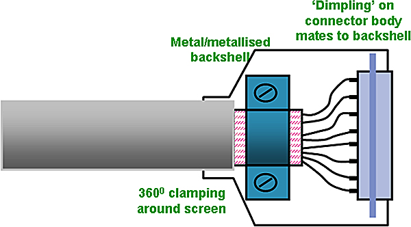
Screened connector
Commercial screened connectors vary quite widely in their form of construction and hence their transfer impedance ZT. Both the method of terminating the cable screen and the method of mating the shells are important. For instance, the principal distinction between so called EMC subminiature D-type connectors and their lesser brethren, are the dimples on the male connector’s shell, and the tin plating on the shells as compared to their non-EMC-dimpled, cadmium passivated relatives. But equally, whatever backshell is used it needs a secure method of terminating to the connector shell and of clampling to the cable screen.
It should be clear that the system transfer impedance defines the overall system screening performance, and this is made up of the sum of the cable transfer impedance and the connectors transfer impedances at either ends. If the connector transfer impedances are substantially greater than the cable, they will dominate. A cable with good transfer impedance is entirely wasted in this situation.
In the case of unscreened connectors, the screen capacitance and pigtail inductance behave as a resonant LC circuit as shown in Figure 6.5.
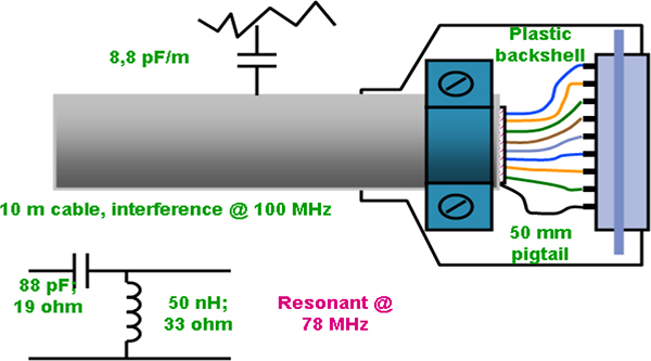
Unscreened connector
If there are signal harmonics at 78 MHz, the screen/pigtail structure can amplify and even radiate this frequency. If the cables are present above 78 MHz RF, the cable/pigtail structure will resonate and induce RF noise in the signal lines – instead of keeping it out. Even if the signal bandwidth is far below 78 MHz, the noise can still swamp the signals.
6.7.1 Cables into screened compartments
Anything that interrupts the current flow will affect the shielding effectiveness. Any discontinuity in the conductive material will interrupt the current flow. Discontinuities are due to a number of factors:
- Joints between structural members and/or panels
- Large openings for windows, access doors
- Small openings for ventilation holes, connectors, controls
The fastest way to destroy shielding effectiveness is to make a hole in it and run a cable through it. Figure 6.6 shows a good practice, but the best way to do it is by using a filter at the interface.
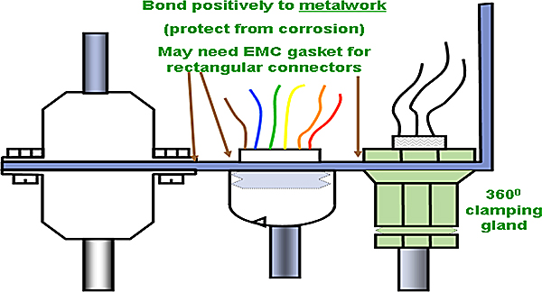
Cables into screened compartments
6.8 Transmission lines
Transmission lines are a means of conveying signals or power from one point to another. From such a broad definition, any system of wires can be considered as forming one or more transmission lines. However, if the properties of these lines must be taken into account, the lines might as well be arranged in some simple, constant pattern. This will make the properties much easier to calculate, and it will also make them constant for any type of transmission line. Thus all practical transmission lines are arranged in some uniform pattern; this simplifies calculations, reduces costs and increases convenience.
Any circuit that consists of series and shunt impedances must have input impedance. For any transmission line this input impedance will depend on the type of line, its length and the termination at the far end. To simplify description and calculation, the input impedance under certain standard, simple and easily reproducible conditions is taken as reference and is called the Characteristic Impedance of that line. By definition, the characteristic impedance of a transmission line (Z0), is the impedance measured at the input of this line when its length is infinite. Under these conditions the type of termination at the far end has no effect, and consequently is not mentioned in the definition.
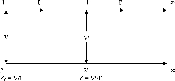
Infinite Line
It can now be shown that the characteristic impedance of a line will be measured at its input when the line is terminated at the far end in an impedance equal to Z0, no matter what the length the line has. This is important, because such a situation is far easier to reproduce for measurement purposes then a line of infinite length.
If a line has infinite length, all the power fed into it will be absorbed. It should be fairly obvious that as one moves away from the input, voltage and current will decrease along the line, as a result of the voltage drops across the inductance and current leakage through the capacitance. From the meaning of infinity, the points 1′ – 2′ of Figure 6.7 are just as far from the far end of this line as the points 1 & 2. Thus the impedance seen at 1′ – 2′ looking to the right) is also Z0, although the current and voltage are lower than that at 1 – 2, followed by a circuit which has the input impedance equal to Z0. It does not matter what the circuit to the right of 1′ – 2′ consists of, provided that it has input impedance equal to the characteristic impedance of the line. Thus Z0 will be measured at the input of a transmission line if the output is terminated in Z0. If the load and source impedances are not matched i.e., if both are not equal to Z0, reflections on the line occur. A non-matched transmission line is ineffective in transferring the signal from source to load and is more prone to emission and immunity problems.
When the frequency of the signal is greater than a quarter wavelength of the signal or multiples thereof and it can fit onto the length of the cable/structure, it is then known as the transmission line. Some experts argue that any structure that is greater than λ/20 of a critical wavelength will start acting as a transmission line (from λ/20 rule). An unmatched transmission line can resonate. This depends on the length of the line and the load. A transmission line can look like a short (from the input side) but physically be an open circuit at the load. It can also look like an open circuit (from the source side), but physically have a short at the load side. If a transmission line in not properly terminated it can become resonant. At resonance the line will either emit or be susceptible to outside interference.

V and I distribution in resonant cables
Figure 6.8 shows the voltage and current distribution in resonant cables. The transmission lines should be handled with great care i.e., there should not be any sharp bends or crushing that increase the losses from transmission lines.
6.9 Cable coupling to radiated field
Cables are most effective at coupling RF energy into equipment at the lower end of the VHF spectrum (30–100 MHz). The external field induces a common mode current on the cable shield or on all the cable conductors together, if it is unshielded. The common mode cable current effects tend to dominate the direct field interactions with half the wavelength of the interfering signal.
A cable connected to grounded victim equipment can be modeled as a single conductor over a ground plane, which appears as a transmission line (Figure 6.9). The current induced in such a transmission line by an external field increases steadily with frequency until the first resonance is reached, after which it exhibits a series of peaks and nulls at higher resonance. The coupling mechanism is enhanced at the resonant frequency of the cable, which depends on its length and on the reactive loading of whatever equipment is attached to its end. A length of 2 m is quarter-wave resonant at 37.5 MHZ, half-wave resonant at 75 MHz.
Figure 6.9 shows a cable shield with one end grounded can be considered as a transmission line and the graph shows induced current increasing with frequency. Keep a watch on the length of interfering frequency vs cable length.

Cable coupling to radiated field
Although covered in detail elsewhere, it is worth noting that the improper use of cables and their shields can be a significant contributor to both radiated and conducted interference.
As shown in Figure 6.10, proper cable/enclosure shielding confines sensitive circuitry and signals entirely within the shield, with no compromise to shielding effectiveness.
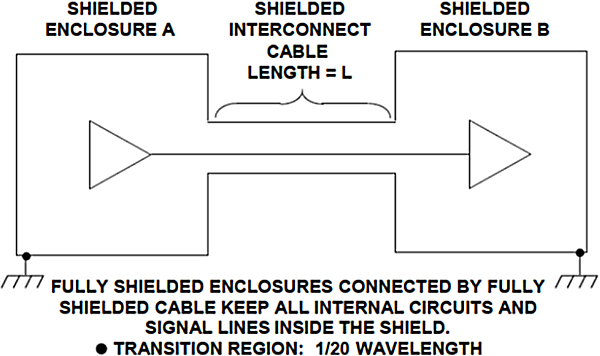
Shielded Interconnect Cables Are Either Electrically Long or Short, Depending Upon the Operating Frequency
As can be noted by this diagram, the enclosures and the shield must be grounded properly, otherwise they can act as an antenna, thereby making the radiated and conducted interference problem worse (rather than better).
Depending on the type of interference (pickup/radiated, low/high frequency), proper cable shielding is implemented differently and is very dependent on the length of the cable. The first step is to determine whether the length of the cable is electrically short or electrically long at the frequency of concern. A cable is considered electrically short if the length of the cable is less than 1/20 wavelength of the highest frequency of the interference. Otherwise it is considered to be electrically long.
For example, at 50/60 Hz, an electrically short cable is any cable length less than 150 miles, where the primary coupling mechanism for these low frequency electric fields is capacitive. As such, for any cable length less than 150 miles, the amplitude of the interference will be the same over the entire length of the cable.
In applications where the length of the cable is electrically long, or protection against high-frequency interference is required, then the preferred method is to connect the cable shield to low-impedance points, at both ends. As will be seen shortly, this can be a direct connection at the driving end, and a capacitive connection at the receiver. If left ungrounded, unterminated transmission lines effects can cause reflections and standing waves along the cable. At frequencies of 10 MHz and above, circumferential (360°) shield bonds and metal connectors are required to main low-impedance connections to ground.
In summary, for protection against low-frequency (¼1 MHz), electric-field interference, grounding the shield at one end is acceptable. For high-frequency interference (¼1 MHz), the preferred method is grounding the shield at both ends, using 360° circumferential bonds between the shield and the connector, and maintaining metal-to-metal continuity between the connectors and the enclosure.
However in practice, there is a caveat involved with directly grounding the shield at both ends. When this is done, it creates a low frequency ground loop, shown in Figure 6.10.
6.11 Useful references
An IEC technical report (IEC 61000-5-2) on the installation and mitigation guidelines is the best reference available.
7.1 Introduction
EMC should be a part of each and every stage of the designing process. Although existing designs can be tinkered with, there is no alternative other than re-designing to ensure compatibility along with provisions for future changes (i.e., to make the necessary changes in the design whenever required). It simply means that there has to be a lot of effort made before the designing process is initiated (Think well before starting!!!). Such an action usually proves to be more effective and cheaper in the long run.
Now the question arises – How to start with a good design? The answer to this is to have knowledge and a better understanding of the hidden components involved in any schematic diagram. Take the example of Figure 7.1; this is the schematic that we can see.

Circuit – what we can see
Figure 7.2 shows the schematic involving hidden components (which we cannot see, but have to be considered for better design).

Schematic – Actual circuit (with hidden components)
Now just see the difference between the schematics in Figure 7.1 and Figure 7.2. The former merely shows the output of an 8 input NAND gate connected to one of the inputs of a 2 input NOR gate (this is what we can see). The latter shows the other hidden components involved.
What are these hidden components?
The answer to this question is the stray capacitance and lead inductance. They can be explained as follows:
- Any conductor in the vicinity of any other conductor gives rise to parasitic (or stray) capacitance.
- Any conductor of finite length has some inductance along its length. This is usually called Lead Inductance.
Thus the presence of these hidden components in Figure 7.1 gives rise to Figure 7.2. These components not only change the look of the circuit but also change the overall operation (or behavior) of the circuit and so these components should never be ignored while designing a circuit. Utmost care should be taken while initiating a design process and all such hidden components should be included, otherwise they may hamper the design when put in practice. The circuit will not behave the way it is intended to, just because hidden components were not considered and one may not even understand the reason for such an unusual behavior of the circuit (even though it works fine on paper). And so it is said – thorough knowledge and understanding of these hidden components is mandatory for circuit designing. Even plain resistors, inductors and capacitors don’t behave as ideal components on a schematic.
7.2 Parasitic in passives
The parasitic elements present in passive components tend to change the role of the passive components and in turn they operate in a way that is not expected.
Some of them are mentioned below:
- Film resistors are capacitive (shunt capacitance of approximately 0.2 pF) and inductance (lead inductance and spiral tolerance); and because of the presence of this inductive and capacitive components, film resistors may resonate.
- On the other hand, wire wound resistors are useless above a few KHz.
- Capacitors have lead inductance as well as internal inductance, and so are mostly above resonance, they are inductive in behavior.
- Due to the presence of parasitic components there are limitations in power handling capability (i.e., the temperature co-efficient change), dI/dt (rate of change of current) capability and dV/dt (rate of change of voltage) capability that is generally found in tantalum objects.
- Stray magnetic fields (as in the case of transformers) and RF pick-ups are the effects that are observed in the case of magnetic components.
7.2.1 SMD features
The following are the advantages and disadvantages of surface mount devices (SMDs).
Advantages:
- They are low profile devices (lower emission).
- Ceramics offers excellent decoupling.
- It consists of fewer parasites (i.e., resistors < 1 kΩ resistive at 1GHz).
Disadvantages:
- They have lower power handling capabilities.
7.3 Clocking
The major source of radiation in digital circuits is the processor clock(s) and its harmonics. All the energy in these signals is accumulated at a few specific frequencies, with the result that the clock signal levels are 10 to 20 dB higher than the rest of the digital circuit radiation. Since the commercial radiated emissions standards do not distinguish between narrowband and broadband, these narrowband emissions should be reduced first – by proper layouts, grounding and buffering of clock lines. Then concentrate on the other broadband sources, especially data/address buses and backplanes, and video or high-speed data links.
It is usually seen that circuits are driven from clock signals whose transition times are substantially faster than required. Undoubtedly there are many high performance circuits where clock timings are critical and transitions must be as fast as possible, but this is not always the case. Wherever circuit constraints allow, slower clock rates tend to minimize harmonic generation. This can be done in three ways: series impedance, parallel capacitance or by using a low-performance buffer.
One possible alternative is a technique more often associated with radio transmission, known as Spread Spectrum clock generation. In this technique a waveform selected for the most even spectral-spreading modulates the clock frequency itself by 1.5 to 2 %. This results in a wider distribution of the spectral energy associated with each clock harmonic so that the level measured in a constant 120 kHz bandwidth falls, between 10 to 20 dB. This is easily achieved without any extra effort made in layouts and without slowing the clock rise times.
7.4 Choice of logic family
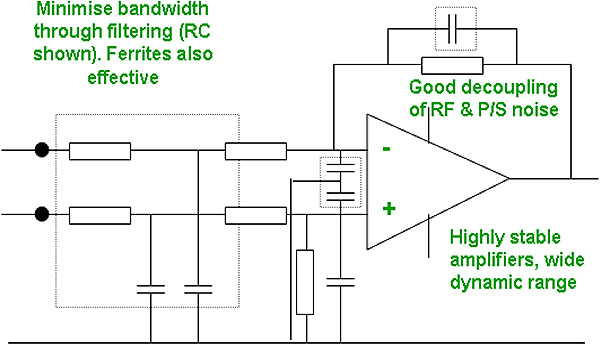
Figure 7.3
Choice of logic family
Table shown in Figure 7.3 shows the logic family along with the corresponding rise time and bandwidth. The bandwidths for different logic families are calculated using the 1/(πtr) formula. It shows that fast logic can generate a very large noise spectrum. The damage (as far as emissions are concerned) is done by switching edges having fast rise times (note that this is not the same as propagation delay and is hardly specified in data sheets; where it is a maximum figure). Using the slowest rise time compatible with reliable operation will minimize the amplitude of the higher order harmonics where radiation is more efficient.
The advice is to use the slowest logic family that will do the job; don’t use the fast logic family. Where parts of the circuit operate at high speed, use fast logic only for those parts and keep the clock signals local. This preference for slow logic is unfortunately against the demands of software engineers for greater processing speeds.
7.5 Design and component choice
Avoid the usage of sockets, as every socket wire increases pin effectiveness as an aerial. If sockets are used considering that the PROMs can be changed (in future course), it is instead better to change the PROM itself to a field-programmable PROM (to avoid the use of a socket). Components with low profiles such as SMDs, BGAs and flip-clips are the best choice.
Fast-switching devices undoubtedly have the highest orders of harmonics, and in turn couple better to adjacent circuits/tracks (that is not required). Use level triggered devices wherever possible rather than using edge triggered devices, which means that rise times are not critical. Even if you don’t eventually use them, try and allow for ferrites or resistors to reduce rise time near critical areas. They can be removed later if not required, but cannot be added later. Keep in mind – high load capacitances means high output current spikes, and that the higher the output impedance, the lower the rise time. Don’t rely on software watchdogs, and use hardware watchdogs for rail monitoring to detect possible power dips and power-outs. Where the rise time of an output is less than the PCB round-trip time, consider using a transmission line rather than a single-ended track.
Many of these requirements appear to contradict existing practice.
- For instance, the lower the input capacitance, the less likely presence of unexpected resonance.
- Higher output impedance means lower energy in the output, and better impedance matching.
- Adjacent power/ground pins simplify decoupling.
- Multiple power/ground pins simplify tracking, and can also help to reduce emissions on signal lines.
- Digital circuits cannot help crowbarring the supply during switching. Choose ICs that minimizes this characteristic.
- Potential resonance can be avoided if the output devices switch cleanly to 0 V and stay there.
- For clock and data lines, balanced (differential) transmission offers many advantages.
- Some components have better diode input protection than others. Check this out if ESD is an issue.
Some products now come with EMC-friendly advice to designers – use it for better outcome.
Here are the principles used for designing –
- Minimize circuit bandwidth
- Maximize signal levels
- Maximize circuit stability
- Isolate susceptible paths
- Use balanced configuration wherever possible
7.6 Analog immunity and demodulation
Generally, analog circuits are not as susceptible to transient upset as digital ones, but may be more susceptible to demodulation of RF energy. This can show itself as a DC bias shift that results in measurement non-linearities or non-operation, or as detection of modulation, which is particularly clear in audio and video circuits. Such a bias shift does not affect digital circuit operations until the bias is enough to corrupt logic levels, at which point operation ceases completely.
Restricting the operating bandwidth to the minimum acceptable level can reduce the level of interfering signal. This can be achieved by input RC or LC filtering, feedback RC filtering and low value (around 10 to 33 pF) capacitors or resistors directly at the input terminals (in reference to Figure 7.4). RC filters may degrade stability or worsen the circuit’s common mode rejection (CMR) properties, and the value of C must be kept low to avoid this, but an improvement in RF rejection (of between 10 to 35 dB) over the range 0.15 to 150 MHz has been reported by including a 27pF feedback capacitor on an ordinary inverting op-amp circuit. The unbalance between capacitances on balanced inputs determines high frequency CMR. An increased input resistance would consequently be too high and might affect circuit DC conditions; a lossy ferrite-cored choke or bead is an alternative series element.
Analog immunity and demodulation
7.6.1 Isolation

Isolation
Signals may be isolated at the input or output with either an opto-coupler or a transformer (Figure 7.5). The ultimate expression of the former is fiber optic data transmission, which with falling costs of components is becoming consistently more attractive in a wide range of applications. Knowing that the major interference coupling route is via connected cables, using optical fiber instead of wire completely removes this route. This leaves only direct coupling to the enclosure, and coupling via the power cable, each of which is easier to deal with electrical signal interfaces. Signal processing techniques will be needed to ensure accurate transmission of precision AC or DC signals, which increases the overall cost and broad area. Isolation is a good way of reducing common mode interference (especially at low frequencies). The advantage reduces as frequency increases (due to the barrier capacitance) until at very high frequencies, there is effectively no such thing as isolation.
Isolation quality is limited by the isolation of the power supplies. All isolation has some parasitic capacitances. At RF, it can be said that signal isolation is simply a myth.

Good practice – CM and DM
It is generally found that common mode signals are the culprits. These can be removed with common mode chokes, baluns and isolation (Figure 7.6). If co-ax is used as shown in Figure 7.7, then it worsens emissions and increases susceptibility.
A specific problem with opto-couplers (that is not suffered by transformers) is that high-level but short transients can couple into the base of the receiving phototransistor and cause its saturation. This actually blinds the coupler, as long as it takes for the device to come out of saturation (which may be several μsecs); the overall impact on the circuit is to evidently stretch the duration of the transient to an extent that is not acceptable. The same effect happens with RF interference, and is due to capacitive coupling directly to the base (Figure 7.8), especially when this is brought out to a separate termination on the package. The problem is less with photodiode couplers, and can be made comparatively less severe with a phototransistor by connecting its base to an emitter with a low-value resistor (definitely at the expense of sensitivity).

Optimizing co-ax
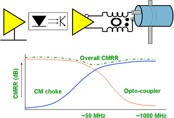
Optimum Common-mode Rejection
7.6.2 Communication
Figure 7.9 shows the ways in which communications can be made. The first one shows co-ax, which is not good to use. Balanced transmission lines are far better to use (in comparison to co-ax). If they are screened, connect screen to earth rather connecting it to 0 V.

Communication – Good, Bad and Ugly
8.1 Introduction
In EMC work, filtering almost always means low-pass filtering. The purpose is to attenuate high frequency components while passing low frequency ones. The purpose of a filter in the context of EMC is to prevent interference from propagating either into or out of equipment via its interfaces. This reduces conducted coupling directly and also helps to reduce radiated coupling if the interference is radiated to or from the cables that connect to the interfaces. Filtering and/or transient suppression, across the appropriate frequency range for every unscreened cable that crosses the boundary, is necessary. This is simple to do for power cables, but for signal and control lines it may pose a problem. For this reason, it is often helpful to partition the whole system so that difficult to treat cables crossing the zone boundaries are kept at a minimum. Screened cables do not need filtering, although surge protection may occasionally be required on internal conductors. However, it is essential to bond the screen to the earth structure at the boundary, whether it is a screen wall or an earth bar. This ensures that the interference currents on the screen are returned to Earth rather than penetrating from one zone to another that would compromise the attenuation otherwise offered at the zone boundary.
Mains filter components are of course rated to withstand the nominal operating voltage plus some safety factor. But the mains supply frequently carries transients that cause an abrupt overvoltage of several times the nominal. Before selecting a filter, the considerations that are to be made are as follows:
- The likely transient environment and
- Whether the anticipated overvoltages will cause the filter too much stress.
When two non-conductive materials are rubbed together or separated, electrons from one material are transferred to the other. This results in the accumulation of triboelectric charge on the surface of the material. The amount of charge caused by this movement is a function of the separation of the materials in the triboelectric series (positive materials give up electrons more readily, negative materials acquire them more readily). Additional factors are the closeness, area of contact, and rate of separation.
The voltage to which an object can be charged depends on its capacitance, and follows the law Q=CV. The human body can be charged by triboelectic induction to several kV. Because a perfect insulator does not allow the movement of electrons, surface charges on an insulator remain in the area within which they are generated, but the human body is conductive and so a triboelectrically induced charge distributes itself over the body. The rate at which the charge will bleed off a body to its surroundings depends on the surface resistivity of the body and its surroundings. This in turn is a function of relative humidity; more the moisture in the air, lower the surface resistivity of insulators and hence quicker the charges bleed away. In practice, since movement is constantly generating charge, there is a balance between generation dissipation that results in a typical level of charge voltage that can be found in a particular environment.
When the body (in the worst case, holding a metal object such as a key) approaches a conductive object, the charge is transferred to that object normally via a spark. This happens when the potential gradient across the narrowing air gap is high enough to cause the spark. It is not mandatory that the target object be grounded. Charge transfer can occur between any two capacitive objects as long as there is a static potential difference between them, and a disruptive discharge current pulse flows.
8.2 Filter types and operation

Filter Operation
From the above configuration it is clear that filtering is essentially the combination of providing a high series and low shunt impedance to unwanted signals. Undocumented characteristics of a variety of components at high frequencies and unanticipated source and destination characteristics can destroy a filter design.
R, L and C are the basic elements in the filter design. Figure 8.2 shows the various simple low-pass configurations and filter circuits are normally made up from a combination of these. Filtering can be as simple as inserting a resistor if the source and destination characteristics permit. The conventional low pass filter is built from two elements: series resistance or inductance, and a parallel capacitor.

Filter types
The choice of resistance or inductance for the series element is usually determined by the signal current that has to be passed – power filters will typically be unable to stand more than a few ohms resistance, but signal filters might easily be able to cope with kilohms. Resistance has an advantage because it absorbs interference energy, does not contribute to resonance, and is of course cheaper and smaller than inductance. Inductance on the other hand can provide high RF impedance with little low frequency or DC loss.
The frequency range that has to be attenuated determines the choice of component types for a filter. Non-ideal components have parasitic impedance that limits their effectiveness. For example, capacitors have unwanted stray inductance and inductors have stray capacitance. High frequency performance demands that these parasitics are minimized, and this puts restrictions on the type of construction. In general, any single component can only achieve a maximum of 40–50 dB of attenuation before its parasitic elements limit its performance, hence high performance filters must use multiple stages. Capacitors create a low impedance to attenuate the interference frequencies and are therefore most effective in a high impedance circuit. Inductors create high impedance to the interference and are most effective in a low impedance circuit.
RC filters are the simplest and the most predictable filter. PI and TEE filters provide low loss to wanted signals and high attenuation to unwanted signals, but are resonant devices and depend on source and destination characteristics for their effectiveness.
8.3 Soft ferrites
One of the most common techniques for reducing both incoming and outgoing RF interference is the application of ferrite sleeves to cables at interfaces. The attractiveness of the ferrite choke is that it involves no circuit redesign, and often no mechanical redesign either.
Current flowing through a conductor creates a magnetic field around it. Transfer of energy between the current and the magnetic field is affected through the inductance of the conductor, for a straight wire the self-inductance is typically 20 nH/inch. In a non-permeable material (such as air or plastic sheath), the magnetic field strength and the magnetic flux density are equal. Placing a magnetically permeable material around the conductor increases the flux density for a given field strength and therefore increases inductance. Ferrite is such a material; its permeability is controlled by the exact composition of the different oxides that make it up (ferric, with typically nickel and zinc) and is heavily dependant on frequency. Also the permeability is complex and has both real and imaginary parts, which translate into both resistive and inductive components of the impedance inserted into the line passed through the ferrite. The ratio of these components varies with the frequency – at the higher frequencies the resistive part dominates and the assembly becomes lossy, so that RF energy is dissipated in the bulk of the material and resonances with stray capacitances are avoided or damped. It is very important to check ferrite impedance vs frequency characteristics for particular applications.
Figure 8.3 shows the effect of ferrites on differential mode (DM) and common mode (CM) signals.

Differential and common modes
The magnetic field produced by the intended go current in each circuit pair is substantially cancelled by the field produced by its equal and opposite return current, provided the two conductors are adjacent. Therefore any magnetic material (such as a ferrite sleeve) placed around the whole cable will be invisible to these differential mode currents. Placing a ferrite around a cable has no effect on the differential mode signals carried within it. A cable will also carry currents in common mode, i.e., all conductors have current flowing in the same direction.
When a ferrite is slipped over a single wire, it attenuates differential mode signals. On the other hand, when slipped over a pair of wires, it attenuates common mode signals.
8.4 Thumb rules
Capacitors work best for shunting noise from high impedance sources, while inductors work best for blocking noise from low impedance sources. From the various filter types mentioned in the above section, it is clear that the capacitor is always connected in shunt (whenever used) and the inductor is always connected in series (whenever used). Here are the thumb rules for various available conditions for unwanted signals:
- High impedance and DM – use shunt capacitor.
- Low impedance and DM – series inductor (both the legs at HF).
- High impedance and CM – identical shunt capacitors with each leg to local earth (usually chassis).
- Low impedance and CM – common mode inductors, all signal legs.
8.4.1 Inductance and current
Inductance (L) reduces as current (I) increases; this is true till the saturation point is reached. Once a core saturates, inductance is lost, i.e., L becomes zero. This has to be taken into consideration in practical applications. If the current is 20% greater than the rated current, then saturation is likely to take place.
Let us take a practical example of an inductor used in a mains filter. Its inductor(s) determines the current rating of the mains filter. These carry a peak current, an excess of which can cause saturation of the choke core, which causes an instantaneous loss of inductance and therefore of attenuation. Power supply current peaks can be thrice the RMS value. It is therefore necessary to measure or calculate the waveform of the current that will be drawn under worst-case conditions to gain information. An inductance saturation curve given by the filter manufacturer shows loss of inductance versus current. The maximum peak current that can be tolerated such that filter operations remain effective can be determined from this curve.
8.5 Filter specification
Before choosing a particular filter design, it is necessary to know the parameters that influence its design. Incorrect filter construction or mounting technique can easily compromise radiated emissions, and immunity. Poor shielding can easily compromise conducted emissions and immunity.
Filters should be located at the zone boundary. In addition to this, filters should be located as near as possible to the apparatus that is expected to be the source or victim of disturbances, to minimize the impedance of the connection. If as a compromise, the filter is positioned outside the protected area, the wiring between the filter and the protected area should be twisted and positioned close to the earthing structure.
The higher the frequency, the more a filter is compromised by RF leakage from its unfiltered side to its filtered side. For many engineers, the ease with which the RF leaks around a filter is surprising. Where an external cable to be filtered enters a shielded enclosure, the filter should be fixed into the metal wall at the point of cable entry and RF bonded to the metalwork all around the aperture it fits into. Through-bulkhead-filters are the best, since they maintain the integrity of the shield, but are often expensive to purchase and install. For mains supply filters, the IEC-320 inlet is the most common commercial style of bulkhead filter for up to 10 Amps, single phase, 230 Vrms.
Most mains filter manufacturers only specify their parts (because of commercial pressure) over the frequency range of the conducted emissions tests up to 30 MHz. The filter becomes less effective above 30 MHz and can compromise the shielding integrity of enclosures. This could possibly cause problems with radiated electromagnetic disturbances. Good layout inside the enclosure will minimize the high frequency coupling onto the internal filtered supply.
A filter must be designed to deal with the mode (DM or CM) that is most relevant to the interference; conversely, a filter that is attenuating the wrong mode will be ineffective. For example, a differential mode (DM) filter configuration will not affect common mode (CM) at all and vice-versa.
The filter designs should be flexible such that last minute changes can be implemented for more effective operation and at the same time, the cost of the design should be under control. All the above-mentioned points should be considered for optimizing the filter opertion.
8.6 Impedance matching
The performance of any filter depends on the impedance seen at its terminal. There are four relevant impedances for a simple single-phase mains filter:
- DM at the mains port
- CM at the mains port
- DM at the equipment port
- CM at the equipment port
All these impedances will be complex and frequency-dependant in real life. Conventionally, filters are specified for terminating impedances of 50 Ω at each end (source-end and load-end), because this is convenient for measurement and is an accepted RF standard. This leads us to a very important point that the filter specifications are optimistic when compared with their performance in reality.
Consider a typical supply filter, installed between the AC power supply and an AC-DC converter of the DC power supply of an electronics apparatus. The impedance of the AC supply can vary by as much as from 2 Ω to 2 kΩ depending on the loads that are connected to it, the nature of the supply transformer and the wiring to the point of connection. The impendence is complex and time- and frequency-dependent. Looking from the filter into the equipment, the impendence of the AC-DC converter circuitry appears as low impendence when the rectifiers are turned on near the peaks of the supply waveform, and as high impendence at all other times. The situation is far from being the matched 50Ω/50Ω setup used to measure filter attenuation.
Filter specifications employ a 50 Ω source and load impendence because most RF test equipment uses 50 Ω sources, loads, cables, and because the main specification standard (CISPR 17) requires this. For most practical uses of filters the specifications obtained by this method are at best optimistic, and at worst misleading. Filters made from inductors and capacitors are resonant circuits, and their performance and resonance can depend critically on their source and load impedances. An expensive filter with excellent 50/50Ω performance may actually give worse results in practice than a cheaper one with mediocre 50/50Ω specification.
Supply filters with a single stage are most sensitive to source load impedances. They can easily provide gain, rather than attenuation, when operated with source and load impedances other than 50 Ω. This gain usually appears in the 150 kHz to 1 MHz region and can be as much as 10 or 20 dB, leading to the possibility that fitting an unsuitable mains filter can increase emissions and/or worsen susceptibility. On the other hand, filters with two or more stages are able to maintain an internal circuit node at an impedance that does not depend very much on the source and load impedances, so they are able to perform better (at least nearly in line with their 50/50Ω specification). Of course, they are larger and cost more.
The easiest way to deal with the source/load impedance problem is to only use filters whose manufacturers specify differential mode (symmetrical) performance for both matched 50/50Ω and mismatched sources and loads. CISPR 17 requires mismatched figures that are taken with 0.1 Ω source and 100 Ω load, and vice versa. Now draw attenuation versus frequency curve consisting of worst-case figures from each of these various curves and use this as the filter’s specification. When filters are chosen using this technique (to try and meet the predicted or actual requirements) their performance can be as good as expected. When the 50/50Ω figures alone are used to predict filter performance the result is often disappointing. The performance will also be different depending on the dominant interference path, CM or DM, since the filter attenuation is different for each mode.
8.6.1 Safety and earthing capacitor
It is usual for mains filters to include capacitors between a phase and earth (the safety); these capacitors suppress common mode noise emitted by apparatus and also reduce the amplitude of incoming transients.
It may even be necessary to take the safety earth out of the RF circuit deliberately, by inserting a choke of the appropriate current rating in series with it. An earth line choke increases the impedance to common mode currents flowing in the safety earth and may be the only way of dealing with common mode interference. This is because it can offer an alternative path for interference currents to invade or circulate within the system, and interrupting this path is a simple way of improving EMC.
From the systems point of view, it will often be the case that several items of equipment will be paralleled onto one mains supply. There is a real possibility that even though an individual apparatus remains within the leakage current limits, the combination will not. Generally earth should be at the same potential throughout the system, but this can result in earth difference voltages.
8.7 Filtering precision and Filter earthing
Differential mode interference is present between the conductors of the pair, and therefore the capacitor must be placed in parallel across the conductors and the inductor in series with just one conductor. On the other hand, the common mode interference appears on both conductors together, returning via the earth connection external to the desired circuit. Balanced transmission provides better immunity and so CM filters can be used.
All commercial filters are housed in metal bodies of some sort, with the body forming the filter’s earth connection. An IEC inlet filter with a metal body installed in a shielded enclosure can only give a good account of itself at frequencies above a few tens of MHz if its body has a seamless construction and its body is RF bonded to the shielding metalwork. The same is true for any other metal-bodied filter. The reason is that any inductance due to a wired earth connection will turn the filter into a high pass configuration. The greater the inductance (i.e., the longer the wire), the lower the frequency at which this becomes significant. Bonding the case directly to the chassis earth is the only sure way to realize a filter’s performance.
Adding further stages to the simple single-stage filter is usually the most cost effective way of improving a filter’s performance. Multi-stage filters are inherently less affected by the extremes of source or load impedance. Especially at AF, two-stage filters may be needed.
The filter is always located at a zone boundary. This is for two reasons:
? The filter is a part of the protection offered by the zone barrier. Locating it at a distance from the barrier would allow cables between the filter and the barrier to break this protection. ? A filter needs a high-integrity earth reference for good high-frequency operations. The zone barrier, which will usually be either a shielding wall in a cabinet or chamber or the entry to an earthing mesh, provides this directly. A large metal plate bonded to the earth structure at the SPC (Single Point of Connection) to a zone can also serve as such a reference.The safety earth (yellow and green wire) is not a reference point at a high frequency (HF) connection. The case’s potential with respect to the reference ground is defined by a complex network of inductances (connected cables) and stray capacitances, which are impossible to predict. As per the thumb rule, the inductance distribution along the track is 1nH/mm; the earthing efficiency determines the filter efficiency. Filters that are bonded to the ground plane are called Shielded; on the other hand, filters that are bonded to earth are called Unshielded.
Figure 8.4 shows the mechanics of filtration. Earthing effectiveness can be nullified by impedance to ground. A proper bonding strap should be used while grounding a filter for high frequency EMI.

Mechanics of filtration
8.8 Filters and shielding
A wire bridging a clean/dirty area can pick up noise from the dirty area and radiate it in a clean area. So cables crossing a partitioning zone need to be filtered. Any cable through a shield offers a potential leak point for EMI. Using a filter in a dirty box shield offers an excellent way of maintaining the shielding integrity combined with the use of filters. Figure 8.5 shows how to mount a screw-terminal filter using the dirty box method.

Mounting supply filters in shielded enclosures
This encloses the filter in an individually shielded, segregated box within the main shielded enclosure. In clean/dirty box arrangement, the dirty box segregation is applied to just one filter. The filter input and output cables in the dirty box must be very short and far away from each other, but even so high frequencies may still leak across and ferrite sleeves may be needed on either or both cables if performance above 30 MHz appears to be compromised.
8.9 Surge protection devices (SPDs)
Surge arrestors are variable resistance devices, whose resistance is a function of applied voltage. They are designed so that they provide a clamping effect when the voltage across them exceeds a certain level.
There are four basic types of SPD:
- Gas discharge tube (GDT) – essentially just a spark gap, slow but very high power and negligible leakage.
- Metal-oxide varistor (MOV) – a bulk semiconductor, fast, less rugged, cheap and low clamping voltage than a GDT.
- Avalanche diodes – a semiconductor device with a zener type of action, fastest but not very high powered, lowest clamping voltages and most expensive to buy.
- Thyristor devices – another type of semiconductor device, slow but will handle high currents.
The GDT and thyristor devices have to be self-triggered before clamping, and during the initial period they let through surge voltages that may be potentially damaging. They also have a foldback characteristics, which means that once they fire-off and are carrying current, the voltage across them drops to well below the level they were previously able to block. Careful design is needed to make sure that, if connected to a source of DC current, they do not remain in continuous conduction, once triggered by the surge. This characteristic is not shared by the MOV and avalanche devices, but their disadvantage is a higher clamping voltage, and hence dissipation, for a given normal system operating voltage.
Figure 8.6 indicates the voltage V/s time waveform of the different types of SPD when exposed to the leading edge of a typical surge test waveform.

Voltage V/s time curves for different SPDs
8.10 Surge protection and data integrity
In properly earth-meshed and light-protected structures, the central volume is least exposed to the effects of lightning. So this is the best place to install the most sensitive apparatus. Installation of electronics should be avoided on roofs, on top floors of buildings (especially tall), near to outside walls, near to outside corners, near to down conductors or near to tall structures (like chimneys). However in all metal structures resembling screened rooms the location of equipment is not generally of any concern. SPD techniques are needed because of the long cable run of telephone and data lines outside building structures and poor earthing techniques.
The general belief is that the interference caused in analog data can simply change the waveshape, which can be filtered and the signal is retrieved without much difficulty. But this is not always true; it will also depend on the frequency of the signal. As far as the software part goes, data integrity should not be taken for granted. It is the role of the software programmer to take into account the data integrity on the line, if the data is send or received over the line. Cyclic redundancy check (CRC) is one of the simplest protocols used.
Typical surge and ring waveshape for testing against the indirect effects of lightning are shown in Figure 8.7 and Figure 8.8 respectively.

Surge Waveshapes
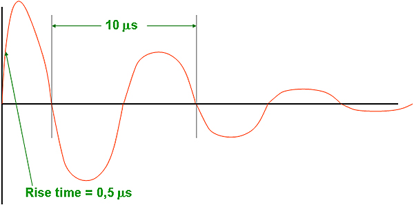
100 kHz ring wave
8.11 Surge protection ratings
Commercial surge protection identifies three distinct zones with differing surge exposure categories: C (most reserve), B, and A (least severe).
- Category C – power conductor outside a structure; supply side of main incoming LV distribution board/switchgear; load side of distribution board/switchgear for outgoing mains cables such as to another structure or external apparatus such as transformers, pumps, external lights, etc.
- Category B – power conductors inside a structure; between load side of incoming distribution board and supply side of socket outlet or fused spur, or within apparatus not fed from a wall socket, or sub distribution boards located within 20 meters cable run of Cat C, or plug-in equipment or fused spur within 20m cable run of Cat C.
- Category A – power conductors to plug-in equipment or fused spur located more than 20 meters cable run from Cat C and/or 10 meters from Cat B (category A may not exist in smaller structures).
These values vary hugely from standard to standard. The IEC 1024 set of standards calls Category C, Zone ‘0’; Category B, Zone ‘1’; and Category A, Zone ‘2’. Figure 8.9 shows the various zones.
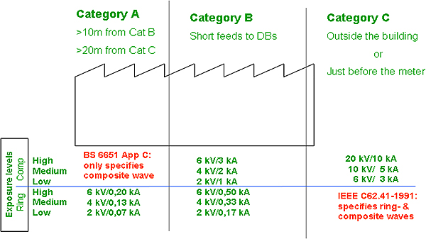
Surge protection Rating
All data/signal cables (e.g. telephone wires) entering a structure from outside are Category C over their whole length, except internal to the structure after suppression by SPDs, since surges in these lines are time-stretched over distance, rather than attenuated as happens with power cables. BS6651 substantially agrees, but suggests an upper limit of 20 kA in Category C in high-risk areas. The exposure levels suggested by BS6651 are based on lightning risk assessment only. If transients of other origin are present, consider upgrading any SPDs and/or specifying apparatus with higher surge immunity. For instance, if in an industrial area the risk assessment suggests that an SPD suitable for medium exposure level is appropriate, the presence of inductive switching transients may make a high exposure level SPD more appropriate. In these circumstances, specialist advice should be sought.
8.12 Surge protection fusing
All SPDs fail eventually, and since the majority use metal-oxide-varistor types (whose failure mode is sustained leaking and finally short-circuiting), those that are placed across power conductors need to be fused. The choice to be made is whether protection of the load (equipment), or continuance of operation is the most important parameter, and is a user’s decision.
If the fuse is in common line that also goes to the load (protected equipment) (see ‘a’ in the Figure 8.10), then the opening of the fuse due to SPD failure will remove the power from the equipment, which may not be acceptable in some applications.
If the fuse is dedicated to the SPDs alone (see ‘b’ in Figure 8.10), when it opens during a surge event that kills the SPD, the load (protected equipment) may be exposed to the remaining parts of the surge and damaged. Afterwards, even if the load (protected equipment) is undamaged, it has lost its surge protection and so is very exposed to the next surge that comes along.

Two distinct fusing arrangements for SPDs
The arrangement of Figure 8.10 (b) is preferred for domestic premises, where no inspection and preventative maintenance of SPDs can be expected, since the continue opening of fuses will inform the user that there is something wrong that he should get fixed. Where a system of inspections and preventative maintenance is in place, and if recent models of SPDs with health indicators are fitted, either fusing arrangement may be chosen.
8.13 Positioning SPDs
SPDs are connected directly across the line to be protected. They are first installed at the equipotential bonding plate, or main earthing terminal in less sensitive structure on all incoming or outgoing conductors that are not directly bonded to the earth at the same place. Other SPDs may be fitted at lightning protection zone boundaries in a similar way within the structure, and some may be fitted at the equipment itself. In all these arrangements, the common need is to keep their lead lengths short and to ensure that their earthing is relative to what is being protected. Connecting to a separate SPD earth is less productive and nullifies protection.
The total let-through voltage of an SPD is the sum of its own voltage clamping action and the transient voltage drop in its connecting leads due to their inductance (usually 1 nH/mm, rule of thumb). For the rate of change of current associated with lightning strikes, if an SPD has an earth lead longer than 1000 mm, greater voltage surges can be let-through to the equipment being protected. For example, in a 6 kV–3 kA test an SPD gave a let-through of 630 volts when it was installed correctly (where a lead’s length is less than 250 mm and bound together), but 2000 mm long bound leads, let-through a total 1,200 V and unbound 2000 mm leads let-through 2,300V. In general, SPDs for lightening suppression should have a lead length of 500 mm or less. Although large diameter wires are slightly better than thinner ones, the most important concern is to achieve the shortest lead length. Binding the leads to/from an SPD also helps reduce lead inductance and in turn let-through voltage. Always make sure that SPD protected cables are segregated from any cables that have not been protected SPDs by at least 150 mm on parallel runs.
When SPDs are correctly fitted to signal and data lines of equipment, their earth bonds will have short connections to the chassis (local earth) of the equipment itself. But the neutral conductor in mains supply is earthed many meters away (for other good EMC reasons), so if the surge is clamped by the signal’s SPD, it will inject a current into the chassis and hence there is a considerable hike in voltage with respect to the remote neutral earthing point. This could create a surge voltage problem for mains supply. A similar problem can occur when SPDs are fitted locally to the equipment’s mains terminals, with the resulting over voltage appearing on its communication cables. So when fitting SPDs to any cables of equipment, it generally means that all inputs, outputs and power cables need to be fitted with SPDs too. Evidently this could be very expensive for equipment with a large numbers of cables.
8.14 Electrostatic discharge
Electrostatic discharge is a source of transient upset that typically occurs when a person or other body that has been charged to a high potential by movement across an insulating surface then touches an earthed piece of equipment, thereby discharging through the equipment. Currents of tens of amps can flow for a short period with a very fast risetime (in the order of few nanoseconds). Even though it may have low energy and be conducted to ground through the equipment case, such a current pulse couples very easily into the internal circuitry and can disrupt its operation. When two objects with a high electrostatic potential difference approach, the air gap between them breaks down and the charge difference is equalized by the current flow across the resultant ionized path. The current route is completed by stray capacitance between the objects and their surroundings, and the inductance and resistance of the path.
The actual current waveform is complex and depends on many variables, which includes speed and angle approach, environmental conditions, as well as the effect of the distributed circuit reactances. At lower voltages a precursor spike due to the local area of the source (a finger or a metal tool) is produced which has a very fast risetime, of the order of a few hundred picoseconds. This spike, although low in energy, can be more damaging to the protection of fast digital equipment than the bulk discharge that follows it, which may have a risetime of 5–15 nanoseconds. The discharge current will take the route of least inductance. If the case is well bonded to ground then this will be the natural sink point. If it is not, or if it is non-conductive then other routes may be via the connecting cables. Because the discharge edge has an extremely fast risetime (sub-nanosecond), stray capacitive coupling is essentially transparent to it, whilst even short ground connectors of a few nH will present high impedance. Apertures in a conductive enclosure will also result in intense local magnetic fields which couple to internal circuits.
The discharge current pulse di/dt and its indirect effects produce the principal effects of an ESD in terms of equipment malfunction. The rate of change of electric field dE/dt when the local static charge voltage collapses can also couple capacitively into high-impedance circuits; in some circumstances into the high static electric field itself, before a discharge happens. This may cause undesirable effects.
The resultant sub-nanosecond transient equalizing current of several tens of amps follows a complex route to ground through the equipment and is very likely to upset digital circuit operations if it passes through the circuit tracks. The paths are defined more by stray capacitance, case bonding and track or wiring inductance than by the designer’s intended circuit. The high magnetic field associated with the current can induce transient voltages in nearby conductors that are not actually in the path of the current. Even if not discharged directly to the equipment, a nearby discharge such as to a metal desk or chair will generate an intense radiated field that will couple into unprotected equipment. Critical areas that can act as sink points for the ESD are exposed metalwork, apertures, front panel components and connectors. Components and apertures can allow a discharge to take place via creepage across a surface to the circuits inside an enclosure, even if the enclosure itself is insulated. The breakdown voltage gradient in dry air is approximately 30 kV/cm but his is reduced considerably across a surface, especially if the surface is contaminated with dirt or other substances.
For reduced ESD susceptibility, circuit ground needs to remain stable during the ESD event. A low inductance ground network is essential, but this must also be coupled (by capacitors or directly) to a master reference ground structure. I/O cables and internal wiring may provide low-impedance paths for the current in the same way as they are roots into, and out of the equipment for common mode RF interference. The best way to eliminate susceptibility of internal harnesses and cables is not to have any, through economical design of the board interconnections. External cables must have their shields well decoupled to the ground structure. Insulated enclosures make the control of ESD currents harder to achieve, and a well-designed and low inductance circuit ground is essential. But if the enclosure can be designed to have no apertures which provide air gap paths to the interior then no direct discharge will be able to occur, provided the material’s dielectric strength is high enough. You will still need to protect against the field of an indirect discharge, though.
Keyboards present an operator interface that is frequently exposed to ESD. Keyboard cables should be foil-and-braid shielded which are 360°grounded at both ends to the low inductance chassis metalwork. Plastic key caps will call for internal metal or foil shielding between the keys and the base PCB that is connected directly to the cable shield, to divert transients away from the circuitry. The shield ground should be coupled to the circuit ground at the cable entry point via a 10–100 nF capacitor to prevent ground potential separation during an ESD event. A membrane keypad with polyester surface material with an inherently high dielectric strength and is therefore resistant to ESD but it should incorporate a ground plane to provide a bleed path for the accumulated charge and to improve RF immunity. The best way to avoid the effects of ESD is to keep plastic enclosures, membrane keyboards, plastic knobs, plastic pot shafts, plastic switch caps, plastic lenses, etc away from each other as much as possible.
8.15 Creepage and clearance
The mechanical design of many electrical products relies on separation distances between live and accessible parts to maintain safety against shock. When such products are placed within screened enclosure, it is necessary to ensure that such separation distances are not compromised. A typical problem might occur when a product in a plastic case with normally sufficient separation between hazardous and safe circuit connections, is bolted to a metal frame inside a screened enclosure; the separation distances from each set of connections to the metal frame may not now be sufficient. A related issue occurs when a plastic case is conductively coated for screening purposes. The original designer may well have relied on the internal case geometry being insulating to maintain safety clearances. Adding a coating can breach these clearances by providing a new conducting path. The dangers of coating also extend to the possibility of flakes of coating becoming detached due to environmental stresses such as vibration or temperature extremes, and lodging in areas where they may bridge critical insulation. Screening is not the only situation in which clearances may be affected: a poorly designed or installed mains filter or surge suppressor can create similar issue.

Creepage and clearance
Dielectric breakdown of air is around 30 kV/cm. With the human body having the ability to acquire a charge of 20 kV, any creepage distance shorter than say 7 mm can lead to a discharge reaching circuitry.
8.16 Shielding
The safety bond, a length of green/yellow wire interconnecting panel and frame or different panels, is familiar to system designers. But it is important to realize that this is not sufficient for EMC bonding. The purpose of a wired safety bond is to prevent different parts of the structure from assuming different potentials and hence presenting an electric shock hazard at power frequencies (it has no other purpose). It cannot give a low impedance connection at RF.
Signals may be isolated at input or output with either an opto-coupler or a transformer. The best example of the former is fibre optic data transmission, which with falling costs of components is becoming steadily more attractive in a wide range of applications. Isolation breaks the electrical ground connection and therefore substantially removes common mode noise injection, as well as allowing a DC or low frequency AC potential difference to exist. However there is still a residual coupling capacitance between primary and secondary that will compromise the isolation at high frequencies or high rates of common mode dv/dt. This capacitance is typically 2-3pF per device for an opto-coupler; where several channels are isolated the overall coupling capacitance (from one ground to the other) rises to several tens of pF. This common mode impedance is a few tens of ohms at 100 MHz, which is not much of a barrier.
An electromagnetic shield is normally made from several panels joined together at the seams. Unfortunately, when you join two sheets the electrical conductivity across the joint is imperfect. This may be because of distortion, so that the surfaces do not fix well, or because of painting, anodizing or corrosion, so that an insulating layer is present on one or both the metal surfaces. As a result of this weak spot (shield joint), the shielding effectiveness is reduced. Shielding effectiveness is defined as the ratio of the field strength impinging on a shielding barrier to the field strength propagated away from the other side of the barrier. It can be expressed as the sum of reflection, absorption and re-reflection losses, and is given by the equation below:
SE (dB) = R (dB) + A (dB) +B (dB)
An electric field impinging on a conductive wall of infinite extent will induce a current flow in that surface of the wall, which in turn will generate a reflected wave of the opposite sense. This is necessary in order to satisfy the boundary conditions at the wall, where the electric field must approach zero. The reflected wave amplitude determines the reflection loss of the wall. Because shielding walls have finite conductivity, part of this current flow penetrates into the wall and a fraction of it will appear on the opposite side of the wall, where it will generate its own field. The thicker the wall, the greater the attenuation of the current through it. This absorption loss depends on the number of skin depths through the wall. The skin depth is an expression of the electromagnetic property that tends to confine AC current flow to the surface of the conductor, becoming less as frequency, conductivity or permeability increases.
8.16.1 Protection at circuit level
Interfaces are particularly susceptible to an ESD event, if they are easily accessible to personnel, or can be approached by the connector of another device carrying a different charge level. In these circumstances transient protection of the interface pins is necessary. For ESD purposes the devices used must be very fast, but at the same time, do not have to carry or dissipate high energy levels. The peak current of an 8 kV discharge event is only 30 Amp for a nanosecond or so. The purpose of the suppressor is to divert current from a susceptible device to a suitable grounding structure, which will normally be the chassis but could equally well be the interface 0 V.
Always treat the critical functions like resets, interrupts, control lines, power monitors, etc with great care. For instance, the reset and edge triggered interrupt inputs are sensitive and glitches have a widespread effects on the processor operation. On almost all the microcontrollers, the reset pin is specified for a minimum active duration of several clock cycles and if it is pulsed for a shorter duration, an incomplete reset occurs, resulting unpredictable operation.
8.17 Signal line protection

Signal line protection (using diodes)
When the I/O line is susceptible to ESD, the line needs to be protected. Usually in case of simple logic devices, diodes are used for protection. They are used for low energy level applications and are not intended for high-energy ones. Such a typical arrangement is as shown in Figure 8.12. Evidently from the figure, it is a simple current limiting arrangement, without any concerns.

Signal line protection (using filters)
Filtering adds another stage of protection by introduction of a filter stage, as shown in Figure 8.13. It should be clear that the filter stage does not modify the data rate, and in case of analog signals, it does not introduce any lags, which can hamper the operation.

Signal line protection (using SPDs)
Another level of protection is by SPDs, Figure 8.14 shows such an arrangement. One of the major issues while applying surge protection is the length of the lead and/or track. Effectiveness is often reduced by the tracks and/or wire inductance. The length of the track should be as short as possible, and the same holds true for lead lengths. Efforts should be made to run the track as if it is a feed-through device.
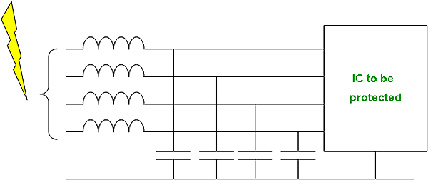
Common-mode filtering
The type of filtering used simply depends on the type of device to be protected. Common-mode filtering is one of the different methods used. For instance, wires from a keyboard (i.e., a group of connections) are often subjected to common-mode transients. For such a case, common-mode filtering is the best method; Figure 8.15 shows such an arrangement.
9.1 Introduction
One of the aspects of electromagnetic compatibility (EMC) is that it is difficult to grasp the techniques involved in making measurements. The highlight of this section of engineering measurements can be summarized as follows:
- Measuring in noisy environment
- RF injection, and
- E and H field probes
9.2 Bench and test laboratory
Bench (basic) equipments such as scopes, signal generators, probes, etc can be used for some EMC measurements. These basic equipments are cheap and generally used for relative measurements only. The other are dedicated equipment such as spectrum analysers, antennas, LISN (Line Impedance Stabilizing Network), shielded enclosures, etc that are generally used for troubleshooting and pre-compliance testing. Basic equipments are generally a fraction of the price of dedicated equipments.
Only calibrated equipment such as those found in a test laboratory can perform absolute measurements. Bench equipments are usually used for indication purpose only or for relative measurements, on the other hand, laboratory test equipments are used for pre-compliance and full compliance testing, and are generally costly. Relative measurements can be performed if a benchmark has already been established. For example, a previously measured level A dB is known, after improving the design and by using bench measurements it was found that the level has dropped down by 20 dB. The estimated level now is (A – 20) dB.
Relative measurements can also be used if a sample (golden sample is generally the word used for such a sample) of the product is available with documented test results. By comparing bench measurements of a new sample with the results of the golden sample, estimation can be made of its EMC performance relative to the golden sample.
9.2.1 Work bench ground plane
It is found that common mode noise currents always create problems in measurements. Every instrument alongwith the test sample should be bonded to a metal plane (of Aluminum or Copper). Figure 9.1 shows a typical work bench ground plane. The instruments (used for testing) and prototype should be grounded to the earth plane by short straps rather than using thin wires. Hook up wires and make them run closer to the ground plane so that the noise pick up is reduced. Isolate prototype live wiring from the ground plane (generally spacers are used for this purpose). Use twisted pair of wires for giving DC supply to the prototype.

Work Bench Ground plane
Using probes
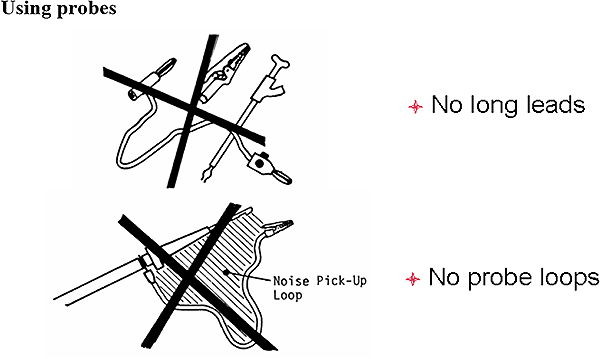
Using probes
Avoid using long leads and loops (as shown in Figure 9.2) while using any oscilloscope probe measurement in the kHz or MHz frequency range as the loop can cut through the electromagnetic (EM) field and may induce noise voltages, which are not part of the measured unit. This may give an uncertain result that is certainly not expected.
9.3 Determining common mode noise
Figure 9.3 illustrates an excellent way of measuring common mode noise. Short the probe tip and crocodile tip (as shown in the figure) to the point intended for measurement. Ideally, i.e., in a noise free system, it is suppose to measure nothing (that means no voltage). But actually what is seen on the oscilloscope is not what is ideally thought. Actually seen is the noise induced by the common mode currents through the test sample and oscilloscope. This is the prime example of common mode noise being seen by the differential circuit (i.e., the oscilloscopes input).

Determining CM noise
To reduce the amount of common mode noise that is seen by the oscilloscope use a ferrite across the probe lead and add a few turns to it as shown in Figure 9.4.
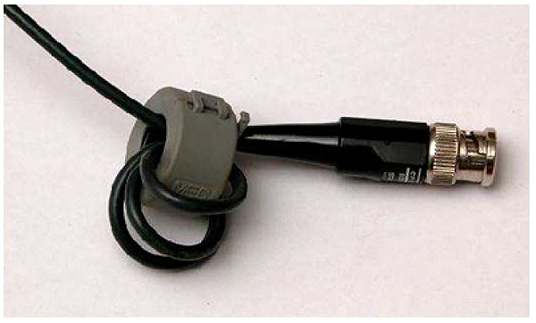
CM filtering on scope leads
Now high frequency common mode currents (that are common to both the positive and negative of the scope lead) see high impedance in the line and therefore reduce the amount of noise flowing through the scope. This works well only into the MHz region, as ferrites do not have high impedance at kHz frequencies.
A much better way of measuring in the presence of high CM noise is to use the differential or a two-probe method as shown in Figure 9.5. Connect one probe tip to the positive end and the other to the negative end of the point intended for measurement. Connect both crocodile clips (i.e., oscilloscope ground) to chassis or plane with respect to which the common mode currents are flowing. Subtract (or invert and add) the two channels for a differential measurement. Always use two identical probes, because if there is any difference in probe impedance then it will cause common mode noise to differential noise conversion and in turn noisy measurements.
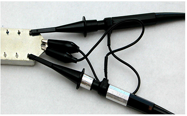
Differential scope measurements
9.4 Field probes
9.4.1 Home made near field probes
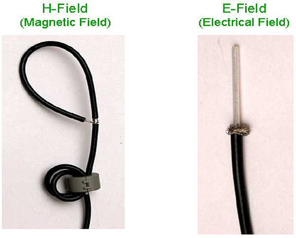
Home made near field probes
A near field E-probe can be constructed from a piece of co-ax as shown in the Figure 9.6. The sleeve is pulled back and a monopole antenna is formed. Although this probe can detect near E-fields, it is not directional. A near field H-probe can be constructed with a loop of co-ax. As shown in the Figure 9.6, the inner is connected to the outer braid and a gap in the ends’ outer braid is left at the connection. This probe is prone to capacitive (E-field) coupling so that a ferrite is used to make sure that only magnetic flux is measured. Both of these probes give only approximate indications and can be best used for relative measurements. The commercial versions of both near field E-probes and near field H-probes are also available.
9.4.2 Sniffer probe

Sniffer probe
A localized sniffer probe should be used when high discrimination is required such as sniffing for high noise traces on a PCB. There are a number of commercial versions available but they can also be constructed in the lab as per the requirement. The probe as shown in Figure 9.7 has got excellent discrimination and can pick up noise from a single component or track. It picks up the magnetic field through the coil and is shielded from other capacitive coupled noise by the tube. The 50 Ω resistor (as shown in the equivalent diagram) matches the source (coil) to a 50 Ω terminated oscilloscope or spectrum analyser.
9.4.3 Home-made current/injection probe
A current probe can be constructed using the home-made H-field probe as shown in Figure 9.8. The current through the wire that is intended for measurement causes the flux to flow through the ferrite and the ferrite concentrates this flux to the centre of the H-field probe, which in turn converts it to a voltage. More windings of either the measured wire or the H-field probe can be used for much higher sensitivity. The fact is that this current probe is only used for rough indication and has a transfer function that depends on –
- Geometry,
- Ferrite, and
- H-field probe
If a signal generator is used instead of an oscilloscope or spectrum analyser, the above set-up can be used as an RF injection probe. Injecting RF currents into individual wires or cable bundles, imitate (i.e., simulate) the effects of these wires being radiated with or being in the presence of high RF fields. This technique (also called BCI, Bulk Current Injection) is more practical than radiation with a RF generator and antenna in a shielded room, and at the same time it is more cost effective.

Home made current/injection probe
Figure 9.9 shows the pictures on a CCTV (Closed Circuit TV) monitor showing the effects of RF being injected with the home-made probe. Noise was injected into the positive power line of a bullet camera that is connected to a monitor. Depending on the frequency, different effects will be seen. This simulates the effects of such a system being in the presence of strong RF fields.

RF injection example – CCTV
9.5 Common mode and Differential mode currents
When using a current probe, care should be taken to distinguish CM (common mode) and DM (differential mode) currents. In a two-wire system such as the supply to equipment, a probe around both wires will measure CM current. To measure DM current, the effect of the CM component can be eliminated as shown in Figure 9.10.

Measuring CM and DM noise
10.1 Introduction
The mains power is a fundamental interface to many if not all functional-modules in a system and compatibility with disturbances that exist on it. So control of disturbance generation is necessary for all such modules. IEC 61000-2-5 (IEC – International Electrotechnical Commission) lists a number of interference phenomena that are associated with propagation via the power supply; many of these are low frequency phenomena such as frequency and voltage variations. The power supply connection also acts as a medium for high frequency disturbances that are difficult to predict and deal with.
The basic characteristics of disturbances on the Power Supply Unit (PSU) may be similar throughout the system. But if the supply is broken into different segments within the system and if each segment has some degree of filtering or suppression isolating it from others, then the supply interface EMC requirements may well be different for different groups of components.
SMPS (Switch Mode Power Supply) generates interference due to switching frequency and its harmonics. It is one of the noisiest units and steps should be taken to make it as quite as possible, this in turn reduces interference propagating to the other units.
The two main issues with PSUs are as follows:
- Emissions: Anything that switches, rectifies and/or is non-linear causes emissions into the power grid/source (AC or DC). These are generally CONDUCTED EMISSIONS back into the power source.
- Susceptibility/immunity: The sensitivity of the PSUs to disturbances such as spikes, sags, over-voltages, etc. from the power source. These are generally CONDUCTED INTERFERENCE from the power source.
10.2 PSUs as noise generators
PSUs are mainly conducted noise generators (Conducted Emissions or Conducted Interference). Power flows from a source (AC or DC) through the PSU to a load, but noise flows from the PSU back into the supply as well as towards the load. The resulting interference may appear as Differential mode (between live and neutral or between signal wires) or as Common mode (between live/neutral/signal and earth). For signal and control lines, only common mode currents are of interest. For the mains port, the voltages between neutral and earth at the far end of the mains cable are of interest. Differential mode emissions are mainly associated with low frequency switching noise from the power supply. On the other hand, Common mode emissions are mainly due to the higher frequency switching components, internal circuit sources and inter-cable coupling.
10.2.1 Supply side noise
Any PSU that creates conducted noise can interfere with any other user (load) on the same grid or rail. There are a number of specifications for controlling this problem; these include the IEC-61000-4 range and numerous military, avionics, medical and automotive specifications. These specifications deal with how much of what supply is allowed to generate (back into the power source) and what it must be able to withstand (arriving through/from the power source).
10.2.2 Load side noise
A PSU not only receives power from a source but also supplies a load. Noise generated on the load rails is not as regulated (from a specification point of view) as that of incoming power. This can become a self-compliance problem if the load electronics are sensitive to PSU noise.
10.2.3 AC Supply and PSU generated noise
Figure 10.1 shows the operating frequencies of the AC supply, switch-mode power supplies and microprocessor clock along with their harmonics. Due to 50/60 Hz rectifiers, thyristor switches, load switching etc., utility grid interference usually occurs in the Hz to kHz region. On the contrary, switch-mode power supplies operate/switch in the kHz region with harmonics extending into the MHz region.
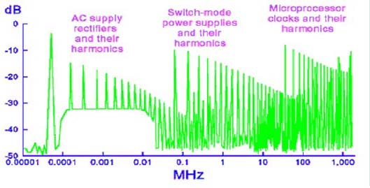
Operating frequencies and harmonics
10.3 Switch-mode PSU as a noise generator
The current drawn by a switch-mode supply contains several noise components. Noise currents are drawn/emitted over and above the usual DC or 50/60 Hz current. These are due to the switching action at fs, the rise and fall time, the duty cycle modulation of the supply and ringing. The major component of Switch Mode Power Supply (SMPS) noise emission is due to the switching frequency and its harmonics. Switching supplies present extreme difficulties by generating interference; typical switching frequencies of 50-500 kHz can be emitted by both differential and common mode mechanisms. Lower frequencies are more prone to differential mode emission while higher frequencies are worse in common mode. Switching waveform asymmetry normally ensures that except at the lower orders, both odd and even harmonics are present. A further cause of broadband noise may be due to reverse recovery switching of the input rectifier diodes.
If the fundamental frequency is well controlled then a spectrum of narrowband emissions is produced which can extend beyond 30 MHz when waveform transition times are fast. A measurement bandwidth of 9 kHz means that individual harmonics can be distinguished if the fundamental frequency is greater than (about) 20 kHz. Self-oscillating converters will normally show drift or modulation due to input or output ripple which has the effect of broadening individual harmonic lines so that an emission envelop is measured.
10.4 Coupling paths, conducted emissions
As in Figure 10.2, where there are high switch-mode frequencies, parasitic capacitance to ground plays a major part. This allows large common-mode voltages to develop relative to ground. In addition, differential mode signals can appear on the supply line or the signal cable as a result of SMPS noise getting through to the signal cable from the supply lines, or directly onto the Live and Neutral from the switching oscillator.

Coupling Paths for conducted emissions
Figure 10.2 shows a typical product with a switched mode supply that gives an idea of the various paths these emissions can take. Differential mode current IDM generated at the input of the switching supply is measured as an interference voltage across the load impendence of each with respect to earth at the measurement point. Higher frequency switching noise components VNsupply are coupled through CC, the coupling capacitance between primary and secondary of the isolating transformer, to appear between L/N and E on the mains cable, and CS to appear with respect to the ground plane. Circuit ground noise (digital noise and clock harmonics) is referenced to ground by CS and coupled out via signal cables as ICMsig (current through the signal cable) or via the safety earth as ICME.
The problem in a real situation is that all these mechanisms are operating simultaneously, and the stray capacitances CS are widely distributed and unpredictable, depending heavily on proximity to other objects if the case is unscreened. A partially screened enclosure may actually worsen the coupling because of its higher capacitance to the environment.
10.5 Power supplies
We are usually made to believe that the key to power supply efficiency is the switching rate but this is not always as true for passive devices as it is for switching devices. It is possible to design for zero voltage or current switching, which helps the EMC enormously, and doesn’t do the stress on switching devices any harm either. Heat sinks can be a problem because of their high surface area. The most effective trick can be to tie them to a rail (directly or capacitively), or use an isolated screen between switch and heatsink and earth them. Transformer interwinding screens can be effective, with some designs using 3 or 5 for best effect, with a combination of connection to earth and rail. Be prepared for some experimentation with these, as well as capacitor connections between 0 V and shields, as well as 0 V and a primary rail. Consider spread-spectrum switching a good option as it does reduce continuous emissions.
10.6 Parasitic components in SMPS
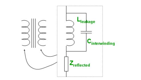
Parasitic components in SMPS
One of the curses of SMPS is their harmonics. Parasitic values start becoming relevant, causing resonance. Any real transformer for example has leakage inductance, interwinding capacitance and sees reflected impedances from the load as shown in Figure 10.3. Ringing occurs once these parasitic resonances are activated (by switching harmonics). These ringing frequencies usually add to the higher frequency current noise components.
10.7 Effects of diodes
Different diodes have different reverse turn-off current characteristics as shown in Figure 10.4. The choice of diode can make a major difference to switching noise. Some snappy diodes can induce parasitic ringing causing high frequency noise. Soft turn-off diode has been developed to solve this problem and is the best option as shown in the characteristics.
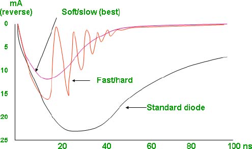
Effects of Diodes
10.8 Improvements from inductors

Improvements from Inductors
Apart from reducing diode switching noise at crossover, inductive input filters help considerably in reducing harmonic currents as shown in Figure 10.5.
10.9 The mains filter
A commonly used mains filter to reduce conducted emissions (noise currents) works especially well for keeping SMPS noise from reaching the mains. A typical main filter shown in Figure 10.6 includes components to block both common mode (CM) and differential mode (DM) components i.e. it incorporates a CM and DM filter.
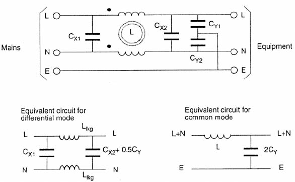
Mains Filter and its equivalent circuits
The common mode choke L consists of two identical windings on a single high permeability core, usually toroidal but sometimes of E-I construction, configured so that differential (line-to-neutral) currents cancel each other. This allows high inductance values, typically 1–10mH; in a small volume without fear of choke saturation caused by the mains frequency supply current. The full inductance of each winding is available to attenuate common mode currents with respect to earth, but only the leakage inductance Llkg will attenuate differential mode interference. The performance of the filter in differential mode is therefore severely affected by the method of construction of the choke, since this determines the leakage inductance. A high Llkg will offer greater attenuation, but at the expense of a lower saturation current of the core. Low Llkg is achieved by bifilar winding but safety requirements normally preclude this, dictating a minimum separation gap between the windings.
The differential mode section filters noise currents between L and N. This is done by the ‘X’ – capacitors and aided by the two ‘Y’ – capacitors in series. The inductor L is a common mode choke. The Common Mode choke has some (parasitic) differential inductance which is used for DM filtering. Common Mode noise between L+N and E is filtered with the common mode choke L and ‘Y’ capacitors.
10.9.1 Common mode capacitors
Capacitors CY1 and CY2 attenuate common mode interference and CX2 is large, have no significant effect on differential mode. The effectiveness of the CY capacitors depends very much on the common mode source impendence of the equipment (Figure 10.6). This is usually a function of stray capacitance coupling to earth that depends critically on the mechanical layout of the circuit and the primary-to-secondary capacitance of the mains transformer, and can easily exceed 1000 pF. The attenuation offered by the potential divider effect of CY may be more than 15–20dB. The common mode choke is the more effective component, and in cases where CY is very severely limited more than one common mode choke may be needed.
10.9.2 Differential mode capacitors
Capacitors CX1 and CX2 attenuate differential mode only but can have fairly high values, 0.1 to 0.47 μF being typical. Either may be omitted depending on the detailed performance required, remembering that the source and load impedances may be too low for the capacitor to be useful. For example, a 0.1 μF capacitor has an impendence of about 10 at 150 kHz, and the differential mode source impendence seen by CX2 may be considerably less than this for a power supply in the hundreds of watts range, so that a CX2 of this value would have no effect at the lower end of the frequency range where it is most needed.
Figure 10.7 is an example of a mains filter. The earth connection is connected to the metal case.

Example of Mains Filter
It seems as if this LC filter is the wrong way around as the noise source (equipment) is on the capacitor side and the load side that should be quiet (mains) is on the inductor side. This is an example of a filter being driven from a high impedance source into a low impedance load.
From a gut feel point of view it can be understood as follows:
- The high frequency noise is shorted through the Y capacitors to earth.
- Any residual noise will see high impedance through the inductor (CM choke) and would rather flow through the capacitor to earth.
10.10 PSU threats
PSU threats are different in magnitude and durations and are as mentioned below:
- Voltage spikes
- Overvoltage transients
- Undervoltage transients
- Frequency variations
- Supply harmonics
A PSU has to be protected against these threats or atleast the consequences of the threats have to be considered.
Most electronic hardware contains elements that are capable of antenna-like behaviour such as PCB tracks, internal wiring, cables and mechanical structures. These can unintentionally transfer energy via electric, magnetic or electromagnetic fields that couple with the circuits. Any EMC situation must have a source of emission and a victim that is susceptible to this interference. If either of these is not present, the problem of EMC never arises. If both the source and victim are within the same piece of equipment, such a situation is known as an intra-system situation and if both are separate items like a computer monitor and a radio receiver, then it is known as an inter-system situation. Since the reduction in the coupling factor is the only way to reduce the interference effects, the knowledge of how the source emission is coupled to the victim is essential. Figure 11.1 shows the potential interference routes that exist between the source and victim.
In practical situations, intra-system and external coupling between equipment is modified by the presence of screening and dielectric materials, and by the layout and proximity of interfering and victim equipment and especially their respective cables. Ground or screening planes will enhance an interfering signal by reflection or attenuate it by absorption. Cable-to-cable coupling can either be capacitive or inductive and depends on orientation, proximity and length.
The PCB techniques described here interact with each other to give improvements that are much greater than each can achieve individually. They mostly improve the PCB’s RF coupling mechanisms, and apply equally well to all types of circuits (analog and digital) and to all the high frequency emissions and immunity phenomena involved with both internal and external EMC.
The PCB-level design techniques mentioned here are well proven to reduce the cost and effort of meeting external EMC requirements such as Federal Communication Commission (FCC) and/or EMC Directive. They also improve internal EMC, a part of which is signal integrity, and help reduce the number of design iterations it takes to get a product to the market. With the advancement in electronic technology (high-clock speeds, improved A/D converter resolutions), internal EMC problems multiply, and the well-proven techniques described here become more important for commercial success.
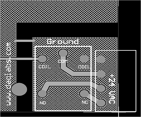
Coupling Paths
11.2 Levels of EMC Engineering Application
Figure 11.2 shows the different levels of EMC engineering application.

Levels of Engineering Application
There are three main areas of EMC Engineering application:
- PCBs
- Circuits/Filters
- Screening
As shown in the Figure 11.2, the PCB is in the center of the 3 levels, this is because circuits on the PCBs are where EMI problems eventually start and end. Grounding techniques are applicable at each level and interconnections between grounds at each stage (level) should be done with great care.
11.3 PCB design objectives
As we know, any EMC situation has a source of emission and/or a victim that is susceptible to interference. In design it is essential to determine the aggressive circuits (source of emission) and victim circuits (circuits that are susceptible to interference). Aggressive circuits are generally high-speed and noisy circuits. On the other hand, victim circuits are sensitive and quite circuits. A circuit node becomes aggressive depending on the maximum dV/dt and/or dI/dt; similarly a circuit node becomes a victim of EM phenomena depending on its signal levels and noise margins i.e. if noise margin is less than sensitivity is greater.
PCB designing is one of the crucial stages and it is essential to spend an ample amount of time on it. A well-designed PCB layout will not only be effective in operation but will also be cost effective. If the process of designing is hurried up it may result in re-layouts and more test cycles that will definitely hike the cost involved in the product. Even if a layer or two is added in the first design itself it is probably not as expensive as trying to force the product into compliance after production. A good PCB layout is the most cost effective option compared to extra filters, components and screening. A proper management system should be laid; life cycle of the product and system costs are the points that are to be stressed.
11.4 Differential mode coupling
11.4.1 Radiated emissions from PCB
In most equipment, the primary sources are currents flowing in circuits (such as clocks), oscillators, etc that are mounted on the PCB. Some of the energy that is directly radiated from the PCB is modeled as a small loop antenna carrying the interference current. Figure 11.3 shown below describes this situation.

Energy radiation from circuits
A small loop is one that is smaller than a quarter wavelength (λ/4) at the frequency of interest (typical example: 1 meter at 75 MHz). When the loop approaches λ/4 the currents at different points on the loop appear to be out of phase at a distance, so that the effect is to reduce the field strength at any given point. The electric field strength varies with the square of the frequency, and is directly proportional to the signal current and loop area.
E = 263 × 10-12 × (f2 × A × Is) V/m …………………..(11.1)
Where, A is the loop area in cm2,
f(MHz) is the frequency of Is the source current in mA.
From the above equation it is clear that field strength increases with the loop area. The loop area is the path traced by the signal current along with the return path. For the field strength to be as small as possible, the loop area should be small, so one of the rules in PCB design and layout is to keep the area covered by the signal current as small as possible (keep the loop areas small). Keep the signal return path as simple and clear as possible. Avoid puzzling and persistent signal paths as they may cover a large unintended area and that in turn results in increased field strength.
The loop antenna not only acts as a source of emission of unwanted noise but can also receive unwanted noise and in turn is the victim of interference. This is one of the main reasons of using gridded grounds and ground planes, which ensure a defined return path for signal currents and avoids any unintentional return paths.
11.5 Common mode coupling
11.5.1 Radiated emissions from PCBs
Differential mode radiations from small loops on PCBs are not the only contributors to radiated emission; common mode currents flowing on the PCB and on attached cables can contribute much more in comparison. The differential mode currents that are governed by Kirchoff’s current law can be easily predicted, in contrast common mode currents on the PCB are not easy to predict. Figure 11.4 shows the return path for common mode currents via stray capacitance (displacement current) to the other nearby objects.

Stray capacitance (via displaced currents)
The full prediction would therefore have to take into account the detailed structure (mechanical) of the PCB and its case, its proximity to ground and to other equipment. The interference current generated in common mode from ground noise developed across the PCB or elsewhere in the equipment and may flow along the conductors or along the shield of the shielded cable. Here even if the cables are longer than λ/20, they will act as an antenna. The common mode noise generally couple through parasitic capacitances.
The equation of field strength in case of common mode is as follows:
E = 1.26 × 10⁻⁴ × (f × L ×ICM) V/m …………………..(11.2)
Where, L is the cable length in meters,
ICM is the common mode current at f MHz in mA flowing in the cable.
Here if the length of the cable increases, the field strength increases proportionally. In PCB design and layout, steps should be taken to reduce common mode currents (minimize common mode currents). Partitioning, filtering, grounding and using planes in PCB design can achieve this.
11.6 Electrical and physical parameters
There are two types of parameters involved in PCB layout (i.e. physical and electrical). Physical parameters are the ones that we build; there are no components involved. The following are the physical parameters involved:
- Copper
- Dielectric
- Traces
- Pads
- Vias
Electrical parameters are the ones that the circuit sees; the following are the electrical parameters involved:
- Resistance
- Inductance
- Capacitance
- Characteristic impedance
Both the physical and electrical parameters together will determine the EMC performance.
11.6.1 Signal Integrity Vs EMC
There is a high degree of awareness among digital designers regarding the problems using high speed signals on PCBs. The problems such as ringing, mismatch and cross-talk on PCBs can cause upsets in digital logic. The general concerns to Signal Integrity (SI) are:
- Power Decoupling
- Ground Bounce
- Reflections
- Cross Talk
A lot of effort is made to design circuits having signal integrity i.e. to be self compliant and extension of this effort will bring us to total EM compatibility. Implementing the best EMC design practices and techniques available will help us achieve Signal Integrity; good signal integrity will make the board more immune to interferences and in turn quieter. The techniques for PCB design are dealt with in the following sections and are mentioned as below:
- Board layout
- Planes and layering
- Grounding
- Decoupling
- Transmission lines
- Multiple boards
11.7 Board layout
Board layout should not begin until it is known whether any shielding and/or filtering techniques need to be physically applied. Once this is decided it is advisable to start the layout process. The first and foremost step is to identify critical circuits, which are divided into two types:
- Aggressive circuits: High speed, noisy, dirty, etc. comes under the category of aggressive circuits. These are the noise generating circuits and cause of generating interference.
- Victim circuits: Sensitive, clean, quite, etc. comes under the category of victim circuits. These are sensitive circuits and are susceptible to interference.
In layout, it is essential to determine the aggressive circuits and victim circuits. On board, keeping the aggressive circuits away from the victim circuits is a part of process called Partitioning.
11.8 Component and track layout
Once circuit partitioning is done, the most noisy or susceptible components in each area should be positioned first, as close to the center of their areas and as far away from cables or wires as possible. Such components include clock generators and distribution (extremely noisy); bussed digital ICs (very noisy); microcontrollers (noisy); switch-mode power transistors and rectifiers and their chokes, transformers, and heat sinks (all very noisy), analog ICs (sensitive), and millivolt level amplifiers (very sensitive).
After the extremely short connections from components to reference planes, digital clock distributions (very aggressive signals) must be the next to be routed, and must be run on a single PCB layer adjacent to a 0 V plane. These tracks must be as short as possible, and even so may need to use transmission line techniques. It may be essential to experiment with component placement to achieve minimum track lengths where clock tracks are made longer than necessary to minimize skew, a Serpentine layout is best.
After this the digital busses and high-speed I/O should be routed next in a similar manner to clock tracks, deferring only to clock tracks and plane bonds where there is incompatibility. Very susceptible tracks, such as those carrying millivolt transducer signals, should also be routed as if they were clock or data bus tracks, although they will always be in a different segregated (separate) area of the PCB. All other types of analog, digital, and power signals should also be routed according to how aggressive or sensitive they are. Where these characteristics are not obvious from a circuit analysis, probing a prototype with a wide-band oscilloscope and/or spectrum analyzer with voltage or current probes will reveal which are the most aggressive, and injecting voltages or currents from a wideband sweep generator will reveal which are most sensitive. A loop probe can be most useful here, being able to inject signals into tracks without requiring connection of external equipment to potentially sensitive areas of the circuit concerned.
Where PCBs have been auto routed additional tracks are found crossing area boundaries, so eliminate them right away by applying more skill to track layout. Auto routing does not generally provide good layouts for EMC purposes. According to Murphy’s Law for auto routers, “Auto routers route to maximize EMI”.
11.9 Areas under control vs outside
The various inside-world areas should be physically separated (both mechanically and electrically) from each other and from the outside-world. From the earliest design phase show the segregated areas clearly on all drawings, usually done by drawing dotted lines around rectangular areas each covering one segregated portion of the circuit. Ensure that this segregation is maintained throughout the rest of the design process including system design, PCB layout, wiring design, mechanical packaging, etc. Segregation should be clearly shown on all system, wiring, and circuit diagrams as it is of great help in communications between electronic designers, mechanical designers, and PCB layout persons and is especially important where people work at different places. Most designing occurs in two dimensions. It is common to find that in the final assembly, a PCB carrying a very sensitive circuit (such as a thermocouple or microphone amplifier) finds itself in close proximity to a noisy circuit (such as a switch-mode power converter), with consequent signal quality problems. Such unpleasant and time-consuming three-dimensional assembly problems should be avoided by detailed visualization of the final assembly from the start, even before the circuits are designed and the PCBs laid out.
Figure 11.5 shows one good partitioning practice applied to a single side PCB
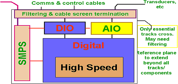
Good partitioning practice
The example mentioned here shows that segregated (partitioned) areas where the outside world interface suppression components are placed along one of the edges of the PCB, as if it acts as a wall between the outside world and inside world. This area would only contain opto-isolators, isolating transformers, baluns, filters, transient absorbers, similar interfacing components but no ICs. It also contains bonding points for the screens of any screened cables and/or for any enclosure shielding. If the PCB were a part of a larger assembly, the segregation techniques employed for best EMC would be just the same. The inside/outside-world interface components are restricted to one dedicated edge of the PCB to restrict all unwanted external currents (e.g. caused by voltage differences in protective earths) to that area of the PCB, and ensure they do not interfere with other circuit areas. Where an effective enclosure shield exists, the inside/outside-world boundary becomes the shielded wall of the enclosure. All of the associated filtering and suppression components and cable screen bonding, must then use a connector panel set in the wall of the enclosure as their reference. A single area for all interconnections is still best. A wider range of PCB mounted screened and/or filtered connectors that can also bond to a metal panel are now available. These parts would be soldered to the PCB reference plane, then electrically bonded metal-to-metal to the wall of a screened enclosure during final assembly, and can be very cost-effective. Narrow channels free from components should be left between each of the segregated circuit areas on the PCB. These should be wide enough for the fitting of a PCB-mounted tuner-can shield, and provision should be made (at least on prototype boards) for bonding such screening cans to the 0 V plane at frequent intervals (every 15 mm) along all edges.
11.10 Reference planes
Tracks, wires, star-grounding, area fills, guard rings, etc, cannot provide an adequate reference for a PCB due to intrinsic reactance and resonance, except at low frequencies (usually below 1 MHz). For example, the thumb rule for the inductance of PCB tracks or single wire is 1 nH/mm. This means that just 10 mm of PCB track has an impedance of 6 Ω at 100 MHz, and 60 Ω at 1 GHz. For this reason, only unbroken areas of metal conductor can provide an adequate reference up to 1 GHz (and beyond), and these are called Reference planes. In a PCB these are usually called power, ground, or 0 V planes, but it is best to avoid the use of the words ground or earth in reference to EMC.
A high frequency reference must have a very small partial inductance, and can be created on a PCB by devoting one layer to an unbroken copper sheet, called a reference plane. A 0 V reference plane would be used as the 0 V or ground-connection for all its associated circuits, so that all 0 V return currents flow in the plane and not in the tracks. Individual tracks have a high inductance; on the other hand planes offer a very low inductance return path that usually offers an instant improvement to many problems. Power planes are created and used in a similar manner for power connections and their return currents.
0 V planes should extend well beyond all components, tracks and power planes. As per the 20H rule: 0 V planes should extend by at least 20 times their layer spacing. High-speed components (such as digital clocks, processors, and memory) and their signal tracks should always be placed near the centers of their segregated (partitioned) areas, well away from plane edges.
11.11 The Image Plane effect
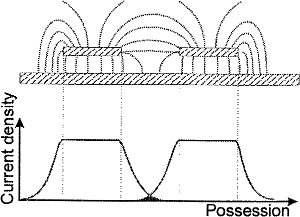
The Image Plane Effect
As shown in Figure11.6, return currents of high frequency signals such as digital signals tend to crowd below the trace if the plane is used. This effect is called the image plane effect. The plane is most effective in reducing emissions if the original PCB suffered from bad layout (i.e., if it included large loop areas). Here the plane can often be brought much closer to the board than the distance that may separate signal and return paths on the PCB. There is a considerable reduction in the effective radiating area, which is determined by the separation between source and image locations rather than the original signal and return.
Another effect of the image plane is to reduce the inductance of each track (including ground tracks) because of the mutual coupling of each track with its image. The reference plane helps in reducing emissions and crosstalk. An added advantage at low frequency is that with a power plane, the DC resistance is decreased. This reduces the common impedance coupling when large amount of power is drawn. The signal line and ground in close proximity behaves like a decoupling capacitor.
11.12 Maintaining plane integrity and gridded ground
Unavoidable gaps in a plane must not merge to create larger ones i.e., continuity in plane is essential. Large open areas cause current concentrations and impedance discontinuities. PCB design rules should size clearance holes so that for regular hole-spacing such as Dual-In-Line packages, the plane webs between holes as shown by Figure 11.7

Hole spacing in PCBs
All 0 V and power connections must bond immediately to their respective planes to minimize their connection inductance. Leaded components must have their through-plated holes directly connected to planes using thermal-break pads as shown in the figure above (sometimes called wagon wheels) to help with soldering.
Surface mounted devices (SMDs) for reflow soldering have to compromise the prevention of dry joints or tomb stoning with the need to minimize inductance of plane connections. Plane connections that do not need to be soldered (typical of the vias for reflow-soldered SMD components) may not need to use thermal-break pads and using solid plane connections instead will reduce inductance. Thermal pads may be required for good soldering.
The logical extension to paralleling ground tracks is to form the ground layout in a grid structure as shown in Figure 11.8.
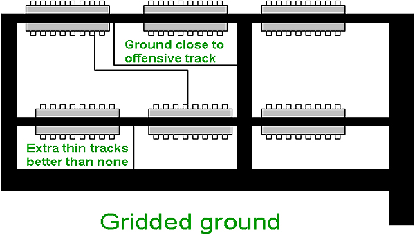
Gridded ground
The grid structure maximizes the number of different paths that ground return current can take and therefore minimizes the ground inductance for any given signal route. Such a structure is well suited to digital layouts with multiple packages, when individual signal/return paths are too complex to define. A wide track is preferred over a narrow one for minimum inductance. The grid layout is best achieved by putting the grid structure down first and then the signal or power tracks are laid out. Aggressive signal tracks (having high di/dt) have to be laid as close as possible to ground tracks to keep the overall loop area small.
This is one of the ground structure configurations that should never be used for any class of circuit. Figure 11.9 shows the comb ground structure in which several ground branches are run from one side of the board.
Even if the signal track is short and direct, such a layout forces return currents to flow in a wide loop. This in turn contributes to increased radiation coupling and to increased ground noise generation. The significant common ground impedance introduced between packages on the board may also cause circuit malfunction. The comb can easily be converted to a proper grid by adding bridging tracks at intervals across the spurs.

Bridging tracks
There may be cases where in plane, layer and even grid is not possible, it is advisable to use the techniques mentioned below:
- Run aggressive tracks directly underneath with a ground track.
- If ground track is not possible, run a 0 V track adjacent to the aggressive track.
- When all else has failed, mount the board directly over the conductive mat like chassis or foiled cardboard.
11.13 Board layering
High speed logic on single sided PCB just does not work that well. In such cases, multi-layer PCB is not an option but it is a necessity. It is necessary to know the frequencies and signal bandwidths above which it becomes necessary to use multi-layer PCB and is mentioned as below:
fclock > 5 MHz (Typical)
tedge < 5 nsec (Typical)
The multi-layer boards have superior noise performance but it has to be compromised with per unit cost, engineering cost and cost of EMC failure. The single most important rule when using multi-layers is to keep all the high frequency signal traces next to a plane and if the trace is not close to a plane, the image plane effect does not work and a layer is wasted.
Burying critical traces between solid planes provides extra shielding and crosstalk control. With a plane between the inner noisy (fast) traces and the outside, extra shielding is achieved. If slower (typical I/O traces) are routed on the outside, the plane reduces crosstalk between the inside and outside traces.
11.14 Layer stacking
To reduce cost, designers often try to design their PCB on a single layer only. This has led to PCBs with a large amount of jumpers on the top of the board. It is very hard to make a single sided device pass EMC standards for noise immunity and radiation. This is because there is no protection for the tracks on either side of the PCB. All the tracks on the single sided board act like antenna (both receiving and transmitting noise). If the designer places a ground plane around the board, it may help, but often this is not sufficient. Only if the design is a low frequency, low power and highly immune to noise, will it pass the EMC requirements. The single sided board, in Figure 11.10, shows two ground planes separated by a small space. Note that the ground planes are connected at the top of the PCB.
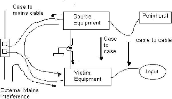
Ground planes
Most EMC experts agree that the four-layer configuration as shown in Figure 11.11 is optimal.

4-Layer configuration
The layers mentioned above are as follows:
- 1 = Microstrip Transmission lines, critical signals
- 2 = 0 V Plane
- 3 = +5V Plane
- 4 = Non-critical signals
The 0 V and +5 V planes that are close to each other create a good capacitor for power decoupling. The critical signals are traced adjacent to the 0 V (reference/ground) plane. Better noise reduction is achieved next to a reference plane as opposed to a power plane. The non-critical signals are of secondary importance with respect to the critical signals and so are still routed next to the +5 V plane. Although more screening can be achieved by burying the signal traces, it is compensated by the fact that the component leads are the main parasitic antennas. Since the components will radiate anyway, burying the traces will not be of that importance. Traces on the microstrip (outside) have better propagation characteristics as compared to stripline (embedded) traces.

8-Layer configuration
The eight-layer configuration is as shown in Figure 11.12. The description of the layers is as follows:
- 1 = 0 V Plane
- 2 = Most critical offset striplines and other signals, routed at 90° to layer 3 to reduce crosstalk
- 3 = Most critical offset striplines and other signals, routed at 90° to layer 2 to reduce crosstalk
- 4 = 0 V plane
- 5 = +5 V plane
- 6 = Non-critical signals routed at right angles to layer 7 to reduce crosstalk
- 7 = Less critical offset striplines and other signals, routed at 90° to layer 6 to reduce crosstalk
- 8 = 0 V plane
The above optimal arrangement behaves according to the following rules:
- For optimal EMC control every signal trace should be routed adjacent to a solid plane.
- The critical signal traces should be as close as possible to a 0V reference plane.
- Keeping the 0V and power voltage planes together creates a good capacitor for decoupling.
- Embedding traces helps with emissions and crosstalk (between planes) but may slow down signal transmissions.
- Using right angles of routing minimizes the coupling between adjacent signal layers.
Stacking arrangements varies from PCB to PCB, but the rules just mentioned above will reduce EMI. This illustration is for the 8 layer stack-up as shown in Figure 11.12. Connecting the layers needs attention as poor layer inter-connections and spacing produce fringe fields. Because of the high frequency characteristics of digital circuits, the ground planes should be connected in multipoint fashion. While interconnecting 0 V layers for digital electronics (i.e. digital ground) care should be taken to have as many interconnections as possible. The distance between the connections should be less than λ/20 of the bandwidth frequency (1/πtr) of the fastest rise or fall time.

Power Plane Fringing Field
The voltage planes are kept smaller than the 0 V reference planes to prevent fringe fields from emitting. Typically the spacing should be greater than 20 times the distance between the planes (also known as the 20-H rule). A single power plane with 0 V planes on both sides is better. There can even be signal layers in between. The best achievable is to stitch the 0 V planes together. This forms a cage that screens all the inside traces. Stitching also helps with the free flow of current between the 0 V planes.
11.15 Grounding on the board
There are two approaches to maintain separate 0 V references for different operational parts of the circuit.
The 1st Approach (as shown in Figure 11.14) says that the ground of each section of the circuit should be separate until they are finally connected at one point on the PCB. This keeps the noise flowing through the analogue ground from being induced onto the digital or signal ground and digital or signal noise being induced on the analogue circuit.
Grounding on a PCB depends on the type of grounds and what needs to be achieved. The Figure 11.14 shows the following ground types or ground areas:
- Power ground
- Digital interface ground
- Analogue ground
- Digital ground with a ground plane
- Chassis or case ground
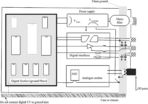
Multiple Ground Type/Areas
Input mains/power should ideally be isolated with a PSU. If not isolated, connect to the rest of the circuit at one point only (low frequency star point grounding). The same goes for the analogue section (low frequency star point grounding that avoids ground loops). Digital interfaces should be isolated or fed through differential op-amps/buffers. Keep grounds from the outside away from internal analogue or digital grounds as cable connections to other circuits can create huge ground loops. The chassis or case connection is usually used as a safety ground or high frequency EMI dump. Use a single connection between chassis and the circuit for safety (single point low frequency) and multiple capacitor couplings to dump high frequency (usually digital) noise.
Analogue and digital circuits usually come together at an A/D or D/A as shown in Figure 11.15. This is the place to connect digital and analogue grounds.

Analog and Digital Ground Planes
The 2nd Approach is exactly opposite to the first; it says that all parts of the circuit should be referenced to a single, unbroken 0 V reference plane. If this approach is chosen, any 0 V tracks would not be acceptable; it is crucial that a high quality, low impedance plane is used. The immediate effect of this construction is that all signal and power return currents flow in the plane so that common impedance coupling between different parts of the circuit is unavoidable. It is only careful layout and the low impedance of the plane that mitigates this coupling to an acceptable level. However mixing sensitive analogue circuits with high-speed digital circuits on the same board is risky but with careful circuit partitioning it can still be successful. As there are no different nodes, the advantage is that there is no opportunity for voltage differences to arise because of interferences between different 0 V nodes.
Finally you are free to use either approach as long as the importance of the decision is appreciated. Separation of grounds removes the threat of cross-interference between different parts of the circuit but requires a careful thinking on placing the boundaries and defining the circuit’s relationship to the chassis. Uniform ground makes it easy to control the ground design but increases the risk of one part of the circuit interfering with another.
11.16 0 V – Chassis Connection
To connect or not to connect and how to connect the chassis/case to the 0V of the circuitry is a difficult question. The following are few points:
- If the circuitry is completely isolated from the case/cabinet/chassis, parasitic capacitances (between circuit and chassis) may build up charge and the circuit can float away. When discharged this can be a safety hazard or damage components. A kilo/mega ohm resistor between chassis and circuit can bleed the charge and avoid this.
- If the chassis is connected to the circuit for safety, use a single star point low frequency connection. This will however not help much with high frequency noise.
- ? When shielding against radiated emissions (or even high frequency conducted emissions), the chassis is used as an EMI dump. Feedthrough capacitors/filters are used to dump high frequency noise to chassis. Capacitors to chassis should be distributed along the digital planes.
- Good high frequency connections/bonding are needed between the capacitors/filters and chassis or the EMI dumps will not work properly.
11.17 Decoupling Capacitors
On PCB level, Decoupling is crucial for EMI control. When digital circuits switch states, they draw currents peaks, and these peaks are seen as noise currents in the power rails. The peaks occur at the clock frequency but also contain a large spectrum of clock harmonics.
Noise current on the power rails can cause not only conducted interference, but since the power rails go everywhere they are effective antennas. Digital designers use decoupling capacitors across the power rails to counteract this problem. Decoupling capacitors supply the ripple current being drawn by the digital circuits so that the power circuit only have to supply DC.
A large decoupling capacitor (typically 100µF) should be fitted where power supplies enter or leave a PCB, and some smaller ones (around 10mF) should be sprinkled around the PCB on a µF per unit area principle, as well as being positioned near to heavy power usage such as microprocessors, memory, and other digital ICs. Using electrolytic technology these bulk capacitors can provide low impedance to about 3MHz. Next, the power supplies to every IC should be decoupled very nearby using appropriate capacitor sizes and types. Where an IC has a number of power pins, each pin should have an appropriate decoupling capacitor nearby, even if they are on the same supply.
The total local decoupling capacitance required depends on the IC’s transient power demands and the tolerances of its DC power rails. The formula C (ΔV) = I (Δt), using the units Farads, Volts, Amps, and seconds covers what we want to know.
ΔV is obtained by subtracting the IC’s minimum operational voltage (from its data sheet) from the worst-case minimum power rail voltage (taking account of initial tolerances, regulation, temperature coefficients, ageing drift, and the voltage drops in the power conductors). ΔV often turns out to be +100 mV.
I is the IC’s transient current demand from its power rail, which lasts for Δt. I and Δt are almost never found in data sheets, and must be measured in some reasonably sensible way with an oscilloscope. An obvious component of I is the device’s output (load) current, but this is often negligible in comparison with shoot-through currents, also known as transient supply current.
Self-resonance in capacitors stops them providing low impedances at high frequencies, with higher values generally being worse. The first self-resonant frequency (SRF) of a capacitor is a series resonance, and a rule of thumb for this is:
fres = 1/ (2π√LC)
Where L = ESL (internal to the capacitor) + the total inductance of any leads + the total inductance of any tracks and/or vias. 1nH/mm may be assumed for leads and/or tracks from a capacitor to the power pins of its IC. The inductance contributed by 0 V and power planes may be neglected when the capacitor is near to its IC. Internal capacitor and lead inductances form resonant circuits and can amplify instead of attenuate power rail ripple and so it becomes important to make sure that nothing resonates.
Decoupling capacitors generally become ineffective at more than 3 times their SRF, as shown by Figure 11.16.

Power rail ripple effect
Digital power current ripple occurs at the clock frequency and its higher harmonics. At these (RF) frequencies, capacitors do not behave as ideal components. Here we have a interesting point to note that the favourite 100 nF capacitor even with no tracks, is effectively useless above 50 MHz, yet it is still often seen in circuits with clocks of 50 MHz and above, where it can hardly do anything to control the fundamental clock frequency, never mind its harmonics. The larger the capacitor value, lower the self-resonant points (the dips in the above capacitor impedance graph). Above this resonant point, the capacitor starts acting as an inductor and is useless for decoupling. Decoupling capacitors should ideally be small (up to a few nF), have low internal inductance and should be connected with short wide tracks (i.e. low RF impedance tracks) to the IC power pins.
A PCB process is available that uses a special dielectric between adjacent 0 V and power planes to increase their capacitance and eliminate the need for most of the smaller values of decoupling capacitors. Three-terminal or feedthrough SMD (Surface Mounted Devices) decoupling capacitors have much higher SRFs than regular two-terminal capacitors, but are more expensive.
One way to achieve possibly adequate decoupling without a power plane is to connect one end of an IC’s decoupling capacitor to its power pin with very short fat track, then connect that end of the capacitor to the power distribution via a thin track (to create some inductance) or ferrite bead, rated for the IC’s current. Three-terminal or high-specification capacitors may be used to advantage so that a high SRF is achieved with a single decoupler. This technique still requires a 0V plane. Where a large number of ferrite beads or expensive capacitors are required, multi-layer boards may prove to be more cost-effective and require less area.
11.18 Transmission Lines on PCBs
With critical switching signals, transmission line design and proper termination need to be used. Transmission lines should maintain characteristic impedance (Z0) from a signal’s source to its load, and unlike all other interconnections does not resonate however long they are. Unterminated transmission lines cause reflections, ringing and cross-talk. Data bus ringing can cause high frequency emissions at the ringing frequency. Termination should ideally be used if the time a signal takes to reach its destination on the PCB is more than half the rise time of the signal. Propagation time in ns/m can be calculated as shown in Figure 11.17.

Propagation time
In the above figures, ɛrr is the relative permittivity of the PCB substrate. The characteristic impedance and propagation time are different for surface microstrip and embedded stripline and is as mentioned above. Striplines are slightly slower than microstrip, but have zero forward crosstalk and much less offboard leakage, so are best for EMC. Databook specifications for output rise/fall times are maximum values, and devices almost always switch a lot faster (assume at least four times faster in the absence of actual data).
The most critical (or highest speed) signals should run adjacent to a 0 V plane, preferably one paired with a power plane for decoupling. Less critical signals may be routed against a power plane where the power plane has been adequately decoupled and is not too noisy (i.e. has been properly decoupled). Any such power plane must be the one associated with the signal’s ICs. Striplines routed between two 0 V planes (one or both of which is paired with a power plane for decoupling) give the best signal integrity and EMC. Transmission lines must not have any breaks, gaps, or splits in any of the planes they are routed over, as these cause sudden changes in Z0. They should also stay as far away as possible from any breaks, gaps, splits, or plane edges, by at least ten times their track’s width. Low crosstalk requires spacing adjacent transmission lines by at least three times their track widths (3-W Rule). Guard traces are tracks next to/over or below a track connected to 0 V and act as a guard or shield and minimises radiation.
Normal FR4 PCB material has a nominal relative dielectric constant (ɛr) of approximately 4.7 at 1 MHz falling almost in a linear fashion with increasing frequency to 4.2 at 1 GHz. Actual values of ɛr can vary by ±25%. Controlled ɛr grades of FR4 are available at little or no extra cost, but PCB manufacturers may not use these grades unless specifically requested. PCB manufacturers work with standard thickness laminations (prepregs), and their thickness should be discovered (along with their manufacturing tolerances) before design starts. The track widths can then be chosen to achieve the required Z0 for the available range of dielectric thickness. Track widths after PCB processing are usually about one thousandth of an inch less than those used on the photoplots. Ask what thickness to add to the drawn tracks to achieve the required finished track widths. For signal frequencies greater than 1 GHz it may be necessary to use dielectric materials other than FR4, such as those used for microwave applications (e.g. Duroid from Rogers Corporation Inc., or a number of more modern dielectrics) as ɛr may be too high for FR4.
11.19 Transmission line termination
Classical RF transmission lines are terminated both at signal source and load by impedances equal to their Z0. Although an ideal and sometimes necessary technique, it halves the received voltage – so most ordinary analogue and digital circuits use low-Z sources and high-Z loads with the line only terminated at one end, to preserve signal levels. Figure 11.18 shows some of the common termination techniques. Classical RF termination is still often used for high-speed signals. Parallel termination at the very far end of a line is used where there are a number of devices spread along the length of the line and they need to respond most quickly and achieves incident wave switching. Figure 11.18 shows the termination resistor connected to the 0 V plane. Parallel termination dissipates a lot of power and may also heavily load some IC outputs.
Terminator resistors
One of the alternative types of parallel termination includes Thevenin. Thevenin uses resistor values designed so that their parallel resistance is Z0 and they would provide a DC voltage at their junction equal to the average line voltage to minimize power dissipation. Thevenin termination needs a properly decoupled power plane at all frequencies of concern so needs decoupling capacitors nearby.
Where a line is driven bi-directionally the compromise position for terminating resistors (series or parallel) is in the centre of the line, so such lines should always be kept very short and may not be able to run as fast as the device speeds may suggest. Series terminations at all possible drivers may be used instead of series termination at the centre of the line, but this may not give good signal integrity unless all the lines concerned are very short. Parallel termination at both ends of the line can give very good performance and allows the highest data rates, but drivers must capable of driving the resulting lower impedances, and power dissipation will also increase.
11.20 Multiple boards and backplanes
Buses that drive several devices or backplanes that drive several boards carry much higher switching currents than circuits that are compact and /or lightly loaded. Products that incorporate a backplane are more prone to high radiated emissions. The back plane is present often where the longest data tracks are. A high speed backplane should always use a multi-layer board with ground plane, and daughter board connectors should include a ground pin for every high speed clock, data or address pin. If this is impractical, multiple distributed ground returns can be used to minimize loop areas. Be careful not to introduce ground loops while connecting daughter boards with each other. A shielded backplane (solid 0V layer) are preferable as long data lines emit. The highest frequency component of a bus should be run closest to its ground return. Clock distribution tracks must always have an adjacent ground return. To avoid introduction of a voltage drop across the power rails (a type of common impedance coupling), use sufficient power pins.
In large systems, use proper I/O circuits on the daughter boards (e.g., buffers). Large backplanes tend to radiate and receive just as interconnecting cables do. Use transmission line techniques and termination where required.
11.21 Interfacing noisy and quite areas
PCBs are interconnected through cables and their interfaces, and these cables act as antennas and noise carriers. This point should be kept in mind while interfacing multiple boards or system. Shield individual areas that are very noisy and/or that are highly sensitive. Never go through a shield without proper common mode filtering. Protect all I/O as transients and noise can damage circuits. Use balanced circuits for their superiority, as far as emissions and susceptibility are concerned. Reduce low frequency ground loops and keep I/O areas separated from the other circuitry, stick to the grounding rules.
Electromagnetic compatibility (EMC) is defined as ‘the ability of a device, equipment or system to function satisfactorily in its electromagnetic environment without introducing intolerable electromagnetic disturbance to anything in that environment’. The environment mentioned in the definition, is the total electromagnetic phenomena in that location.
It is necessary to know the importance of EMC for any product, which is possible only in its absence. Effective EMC requires that the system is designed, manufactured and tested considering the operational electromagnetic environment. Before going to the steps and techniques involved in EMC management, it is important to know the issues affecting EMC that makes EMC engineering management as important as any other aspect involved in the process, it cannot be overlooked.
In modern technology, the usage of microprocessors has increased alarmingly which is a major concern as far as EMC is involved. Such devices are responsible for generating Radio Frequency Interference (RFI) and at the same time they themselves are susceptible to much interference. On the other hand, the use of moulded plastic enclosures in place of metal chassis and cabinets has reduced the degree of protection involved in housing of the circuits.
12.2.1 Malfunction of systems
Digital bus architecture in which many signals are multiplexed on a single bus under software control (as in processor based systems) is preferred over hard-wired logic (as in relay logic). Such a structure (digital) is more prone to interference because a low level of energy is sufficient to induce change of state. A random pulse may or may not affect the operation because it depends on its timing with respect the clock, data transmitted and a program’s execution state, it is impossible to predict the effects of the interference. If the interference exceeds the tolerable limit (in this case logic threshold), the processor operation will be disrupted which leads to system failures.
Phenomena
Electromagnetic phenomena expected to interfere with systems are given below:
- Power supply dips, surges, fluctuations, interruptions;
- Transients on power supply lines, control lines and signal lines;
- Electrostatic discharge (ESD) from a charged object;
- Low frequency magnetic and/or electric field;
- Radio frequency fields coupled within the equipment or through connected cables.
Software
Many times malfunctions due to software are confused with those due to EMI. In real time systems, critical software execution along with transients of external conditions causes operational failures that lead to system crashes, incorrect data and faulty operation – identical to those induced by EMI. This makes it difficult to distinguish faulty software from poor EMC practices.
Interference with radio reception
In the radio spectrum, if the interference is present on some wanted channel then that channel will be destroyed if the interference is of same or greater magnitude. Equipments should be immune from the local fields of intentional radio transmitters and the unintentional emission must be limited to protect the operation of intentional radio receivers; from this it is clear that the complementary aspects of EMC (emission and immunity) address two different issues.
Certain industrial, scientific and medical equipments (collectively known as ISM equipments) generate high level of RF energy that is not used for communication and also produces interference. Co-channel interference is caused when two radio systems are allowed to use the same frequency on the basis that there is sufficient distance between the systems. But due to abnormal propagation, interference occurs that is often regarded as an EMC issue.
Disturbance on mains supply
Disturbances caused by voltage variations, fluctuations and interruptions, waveform distortion, transients and surges leading to malfunction in systems are referred to as EMC issues.
The mains distribution network like main signaling (MS) superimposes signals in the frequency range of 3 kHz to 150 kHz on the mains which is the also the best efficiency operating region for electronic power converters like switch-mode power supply (SMPS), variable speed motor drives, induction heaters, etc. This supply in turn is used by the supply industry itself and also by the consumers.
Other EMC issues
All the above-mentioned issues directly affect the product design but there are some other issues that are necessary to be known. They are as follows:
EEDs (electro-explosive devices) and flammable atmospheres
The incident RF energy results in the ignition of flammable atmospheres in petrochemical plant while EEDs are connected to their power sources for detonation, which can behave as antenna.
Data security
Security of confidential data is another aspect of EMC. Low RF emission from the data processing equipments may be modulated with the information. These signals can be detected by the third party and can demodulate for their own purpose.
Electromagnetic weapons
An intentional broadband radiated pulse can be generated and it can upset all the susceptible electronics within a certain range. This can be used as a weapon against enemies.
12.3 Wait and it’s too late
The control of EMC is necessary for financial benefits to both suppliers and users. EMC practices should be implemented from the designing stage to assembly and installation. It should not be left at any stage, especially designing which is one of the crucial stages and most of the mistakes tend to happen during this stage thinking that it can be compensated at later stages where it will be too late to handle. EMC techniques need to be applied not from the designing but from the very beginning (even at the project specification and tendering stages) to gain higher benefits and lower risks. The correct application of EMC techniques will reduce the project duration, ensure reliability and reduce commercial risk.
12.4 How to manage EMC
It is mandatory to control and manage EMC activities and so it is essential to have management structures defined for EMC activities. This is achieved by establishing an EMC control board that will look after the effective execution and schedule of the EMC control plan. Procurement of equipments is one of the main concerns of the control board’s activity and they should have the requisite authority. For system development, many stages are involved and only after the successful review of the previous stage, progress to the next stage is allowed. The control board must have the authority to define and test various module-level requirements to ensure system level compatibility.
The control plan is divided into three sections viz., EMC risks, design practices and project reviews and control stage.
EMC risks
EMC risks have three aspects to be considered. They are as follows:
Identifying the EMC issues
- Electromagnetic environment that will be suffered by the system
- System interface requirements
- Module level immunity and emission
- Power supply compatibility
- Earthing and isolation
- Cable issues
Listing of probable sources and victims of Interference
The components that are generating interference are sources while those that are susceptible to interference are victims, both are critical as far as EMC is concerned. Identification of such critical components is mandatory and special attention should be given to such components throughout the process.
Control of assembly and installation
Observation of a number of assembly and installation practices is required in maintaining EMC. These include:
- Protection zones in the installation
- Structural components of racks and cabinets should be bonded.
- Proper termination of cables
- Layout, separation and routing of cables
Design practices
Select components and circuits considering EMC issues
- Use RF decoupling capacitors near to ICs
- Use buffers to reduce fan-out on clock circuits
- Use filtering for all analogue inputs
- Minimize signal bandwidth
- Use high immune logic
- Incorporate every microprocessor with watchdog circuit
PCB layout
- Ensure proper signal return paths
- Keep sensitive circuits away from interference paths
- Incorporate ground and power planes such that they do not overlap
- Minimize enclosed loop areas in sensitive circuits
- Minimize component and track leadout lengths
Grounding
- At the product definition stage, design and enforce the ground system
- Ground is considered as current return path and not a 0V reference plane
- Keep earth leads short with specific geometry
- Provide decoupling for all interfaces and provide clean ground area
- Avoid common ground impedances
Filters
- Optimizing the mains filter
- Filter all the input/output lines
- Ensure proper ground return path for each filter
- Ensure filtering for interference sources like motors
Cables
- Prevent parallel runs of signal and power cables
- Use twisted pair for balanced and /or high di/dt lines
- Terminate high frequency lines with correct impedance
- Avoid resonant lines wherever possible
Shielding
- Depending on the frequency range, determine the type of shielding
- Extra shielding for sensitive areas
- Ensure separate panels are bonded along their seams
Project management
EMC design reviews, control stages and checkpoints are incorporated in the project management scheme.
- Preliminary design review
- Design testing
- Detailed design review
- Pre-compliance confidence testing
- Final design review
- Compliance test or certification
- Responsibility for Declaration of Conformity
- Production quality assurance
12.5 Levels of compliance
There are four levels of compliance. The block diagram shown below shows the different levels of compliance with increasing need of EMC Engineering management. The arrows indicate the increase in level and in turn greater need for EMC Engineering management.

Levels of Compliance
Self compatibility
This is the lowest level in the compliance level block diagram. Here no EMC design rules are applied and the product is just made functional.
Minimum engineering/in-house standard
At this level basic EMC design rules are applied to meet the minimum specifications of the product. An impressive product is obtained with improved functionality.
Contractual compliance
Here more stress is laid on EMC Engineering rules for better design to attain the required specification. Designing is done to attain definite specification with the EM environment into consideration. Testing is to be done at module-level and it is mandatory throughout the process.
Special requirements
Here the EM environment is harsh such that it dominates the products operation. It is very difficult to set standards for such cases.
12.6 EMC lifecycle
Envisaged specifications for a product
In EMC lifecycle, there should be a clear view of the specifications like environment, critical equipments, safety aspects and standards. The environment is the Electromagnetic environment in which the product will be surviving. The critical components and equipments are those that are susceptible to EM environments and the others that are sources of interference. Listing of such components is necessary and should be looked after seriously.
Safety is one of the major concerns as there should not be any hazard to people and property because of incorrect implementation methods. Safety questions should be invariably raised, which should include the issue of safety in the face of internal and external interference. In more complex systems, it becomes more difficult to implement safety functions and so the question of the immunity of the electronic devices should be raised.
Standards should be defined and the process implementation should be such that it leads to attain the defined standards. The existing standards fall into a number of categories as listed below:
- RFI: intended to protect the radio spectrum from specific interference sources.
- Mains emission: intended to protect the low-voltage power distribution networks.
- Product and Industry specific: to ensure the immunity from interference of particular types of product, or to regulate emissions from equipment that will be used in a specific environment.
Design philosophy
The design should meet standards that can be assured by implementing the best design practices. These practices involve grounding, PCB layout, power supply, circuit techniques, etc. Implementing a strategy of EMC compliance within a company is much more than just ensuring that the designers make certain their designs meet standards. EMC awareness (like quality and safety) needs to spread throughout the company to be effective. Each department must know its role in maintaining a product’s EMC. This will put pressure on the previous department in maintaining EMC strategy, which will lead to a better product in terms of EMC.
Block level
As we know that integration of different modules results in the final product. To obtain a better product, it is necessary that all the modules are perfect. It is very much necessary to check the operation of each module individually and ensure EMC compliance. So before going for actual implementation, it is advisable to simulate each module to ensure that it meets the standards.
As a part of test plan, it is likely to include tests on individual components of the system (ie., module-wise testing). Some tests require that each module be tested in conjunction with the other components to which it will be connected in the final installation. Each module should meet relevant standards such that in conjunction with all the modules (ie., entire product) meet the intended standards.
Carry through to QA
The EMC compliance does not stop when the product moves from the design to the production stage. The EMC performance of a product in a series production might differ from the product when it was tested. The reasons are as mentioned below:
- There may be different build states as a result of engineering design changes.
- The production tolerances will vary the emission level from the noise sources or the susceptibility of the victim circuits.
Within a company that has recognition of ISO 9000, procedures can be set up and documented to ensure that EMC is maintained during production. These procedures will depend on the exact knowledge of what aspects of production processes are important to EMC. The company’s operation can be revised in the below mentioned ways:
- Determination of all EMC critical parts, assembly, installation and processes by the design authority.
- Clear marking to parts and work instructions to indicate they are critical and a procedure to invoke the EMC authority when changes are required.
- Optimizing the level of in-house testing for early detection of variations.
Complaints in any of the cases should be analyzed and investigated. It cannot be overlooked at any stage and should be continuously looked after for better outcome.
12.7 Life-cycle flow chart
EMC engineering should be part of product life cycle processes like quality. Below shown is the life cycle flow chart of a product.

A typical flow chart
12.8 EMC in context
EMC awareness needs to be extended horizontally and vertically throughout the company for its effectiveness. Everyone should be involved in maintaining a product’s EMC with a clear knowledge of its role. Generally people have illusions regarding their roles thinking that it will not make any difference to the product’s EMC if they don’t fulfill their roles. It is the role of the top-level management to clarify individual roles along with the importance focusing on the product’s EMC. The consequences should also be made clear, in case their role is not fulfilled with responsibility. The correct application of EMC knowledge and techniques will reduce project timescales, ensures reliable operation and reduces commercial risks. If EMC techniques are employed from the very beginning of the project (even at the project specification and tendering stage), they will yield great benefits in terms of cost and low risks.
The specifications to be attained should be decided and listed, the design and implementation should lead to attain the defined specifications; meanwhile provisions should be made in case of iterations (changes) to be made, the design should be flexible to undergo changes.
12.9 How much effort?
Guiding an individual project through EMC compliance can absorb (if it is done thoroughly) between 10 to 20% of the development cost. Thus for every 5–10 design engineers, there should be at least one EMC engineer. There should be a separate EMC department in case of companies with large development departments and a wide range of products. On the other hand, for small companies a retained consultant may best do the job.
The first step of any company implementing an EMC control policy is to appoint an EMC co-ordinator; this is a design engineer who has more knowledge than anyone else on RF topics. The magnitude of task that is to be performed by EMC co-ordinator is appreciable and the powers to be delegated to him/her should be sufficient to deal with all the issues that will arise. In particular, the distinction between engineering decisions and legal or business decisions must be maintained, or else the co-ordinator’s function must include legal and business authority and his/her training must reflect this responsibility. Some of the job functions expected of EMC co-ordinator are as follows:
- Keep abreast with new developments in EMC
- Establish co-operation with all departments on EMC issues
- Control EMC-related changes
- Interpret EMC standards requirements for company’s product range
- Advise and oversee design processes
- Device schedules, tests, and control plans
The EMC coordinator should be present at every design review and should also be included in the sign off for the review. It is his/her responsibility to question each and every design decision that may have an implication for the product’s EMC profile. Its responsibility extends beyond designing and manufacturing of a product. In the field, service technicians repair equipments. Similarly large equipment and distributed systems are build onsite/offsite by production fitters and installers. These groups will either need to have knowledge of EMC or will need to follow tightly controlled procedures. Purchasing may also influence the product’s EMC and so components should be procured to EMC specification. EMC managers should maintain a balance between awareness and procedures in all these cases.
12.11 Design practices
Anyone can’t just become an EMC coordinator, it requires a lot of skills and thorough knowledge of electronics. Theoretical knowledge is important and at the same time the implementation knowledge in designing and manufacturing a product is equally important. The most important role of an EMC coordinator is to maintain an EMC profile throughout the product life cycle. It is his/her job to understand the environment in which the product has to function with the relevant EMC phenomena. The laws involved in EMC have to be properly understood and the relationship between the product and pre-defined principles has to be found for better outcome. As we know designing is one of the most crucial steps in EMC, but does not mean that after the design process, we can relax assuming that the EMC issue is overcome in designing. It requires best design practices and reviewing EMC issue throughout the product life cycle and not just restricting to the design phase.
12.12 EMC engineering implementation
EMC Engineering Implementation
EMC Engineering should be implemented throughout the development/production cycle. Legal and contractual requirements are used to define the product specification and should clearly state the EMC requirements. Design is an iterative process where EMC pre-compliance testing and evaluation is mandatory. The control plan is a master document that describes the complete EMC control process. Emphasis is usually placed in design rules for compliance. Test plan and test result are part of well-controlled EMC process. During production, items should be sampled and even re-tested (if required) to ensure compliance.
12.13 Project management
It is necessary to have a project management defined for the EMC activities. The responsible person is usually EMC co-ordinator. The points that are to be considered in EMC project management are as follows:
- Procurement responsibility.
- Reporting structure.
- Responsibility of design changes.
- Planning and scheduling of control program, including resources.
- Review and co-ordination procedures.
Definition of the intended environment along with critical circuits is done by the co-ordinator. Test results from equipment level EMC test are integrated to analyse and determine the effects of acceptable degradations. Each stage is reviewed and tested individually for better performance.
Compliance certification can be of two types:
Self certification to standards
In self certification, a manufacturer can find a suitable standard or set of standards that can be applied to the product. These standards are relevant for its intended environment, then he/she is able to apply for these and having done so, he /she is free to make a declaration, apply the CE mark and market the product. There is no third party involvement required.
Use of Technical Construction File (TCF)
In case where the manufacturer is not willing to apply harmonized standards in full, the EMC Directive allows this option. The primary purpose of the Technical Construction File is to support the manufacturer’s declaration of conformity to the essential requirements.
12.14 Need for control plan
Within a company that has attribute to ISO-9000, procedures can be set up along with documentation to ensure the EMC is maintained during production. These procedures will depend on a thorough knowledge of what are the aspects of production that are important to EMC.
Generally outside consultants are involved, but in case when they leave there is no expertise left, because of this there is no succession of expertise and experience to guide the process. The only help possible in this case is the software packages that store the steps taken to date but no in-house knowledge and experience. This brings the need to balance the outside expertise and knowledge with the in-house. There should be succession of knowledge throughout the company such that the company is never lacking the knowledge and expertise.
Documentation becomes crucial, as it is one of the best sources of reference and should be maintained for future references. The documents should include histories of design philosophies, corrective actions taken, why certain approaches were adopted, who came up with particular idea, how effective they were correcting the situation and which approaches didn’t work. At least by referring to these documents one can have a clear idea of the best approaches that has lead them to success and the designs that should never be used in future. A control plan is such a dedicated document that sets out the how of reaching EMC compliance of each product.
12.15 Test plans
Before actual implementation of any process, it is very much necessary to decide and lay the test plan. Once implemented, testing is done as per the test plan and so test plan becomes very crucial part of the activity. Any changes made should be followed by a test; it should not happen that the changes are made without testing for the same. Documentation done during design stages can prove very much helpful during future stages as it includes the following information:
- It includes the reason why certain steps were taken, and who came up with ideas for that steps.
- It also includes which steps didn’t work and so these steps should not be further included in future designs. This can be used for future reference.
It is necessary to state why the tests are to be performed. There should be specific test objectives:
- To meet legal standards: it will be necessary to be legally permitted to place the equipment in the market.
- To meet voluntary standards: to have competitive advantage.
- To meet contractual obligation: EMC performance has been written into the procurement contracts for the system or equipment.
Actual tests that are to be performed should be clearly mentioned:
- Voltage levels and frequency ranges to be covered: these are normally specified in the standards that are chosen.
- Test equipment and facility to be used: if it is external test house is used, they will determine the instruments required performing the required test and if the tests are done in-house, it is your responsibility to determine the instruments.
- Location of test points: the number of line directly influences the test time; the standards may define which lines should be tested. In some cases you can test a single representative line and claim that it covers all others of the same type. The position of the test point can be critical, especially for ESD application and must be specified.
- Equipment Under Test (EUT) operating modes: if there are several operating modes then you may be able to identify a worst-case mode which includes the majority of operating scenarios and emission/susceptibility profiles. It has direct influence on the testing time. The rate at which a disturbance is applied or an emission is measured also depends on the cycle time of the specified operating mode.
- Test schedule: the order in which the tests are applied and the sequence of the operating modes should be specified.
Criteria for determining locations of monitoring or injection points and exercising software:
- It is important and necessary for both you and subsequent assessment authority to know why you have chosen a particular point on the EUT for testing. These are often specified in the chosen standard, for instance mains lead for conducted emission. But e.g. the choice of ESD application points should be supported by an assessment of likely use of the equipment and/or some preliminary testing to determine weak point.
- The EUT may benefit from special software to fully exercise its operating modes and in case if it is not stand-alone it will need some ancillary support equipment. Both of these should be calibrated for the purpose. If the support equipment is housed in a separate chamber it can be interfaced via a filtered bulkhead, which will reduce accidental emissions and isolate it from the disturbances applied to the EUT. Specify this filtering arrangement.
Requirements of test facility
- Environmental conditions: requirements for temperature, humidity, vibrations, etc.
- Safety precautions required: e.g. if the EUT uses ionizing radiations or extra high voltages, is dangerously heavy or hot, or if the tests require high values of radiated field.
- Special handling and functional support equipment: large turntables, hydraulic or air/water cooling services, forklift trucks, etc.
- Power sources: AC or DC voltage, current, frequency, single- or three-phase, VA rating and surge current requirement, total number of power lines.
- System command software: is there any special requirement of software to be written to integrate the test suite with the EUT operation?
- Security classification.
Reporting and Report evaluation
- It can range from a test house certificate that states whether the EUT did or did not meet its specification, to a detailed test report which includes all the test procedures and results. For complying with the EMC Directive, you need to know whether you want a certificate of compliance with an EN standard or a report for insertion into a technical file.
- Computation of safety margins: the test results will primarily include the levels of EUT emissions or the levels of disturbance at which susceptibility effects occur. There should be an accepted way of deriving safety margins between these levels and specification limits, determined by know measurement uncertainties and the operational parameters of the system in which the EUT is placed. These margins are necessary for interpretation of test results.
- How to deal with ambient signals: in emission testing, the signals that are present in the test environment may be of a sufficiently high level to mask the EUT emissions. If this is the case, some emission standards define the procedure to be followed.
Interfacing with test authority
- Test authority should be continuously interacted during testing and they should be involved in all the discussions regarding testing. Agreement for each and every phenomenon to be tested along with reporting should be interfaced with the test authority. There should be involvement of test authority in scheduling of activities.
12.16 Test reports (immunity)
When immunity tests are performed, it is essential to be able to judge whether the Equipment Under Test (EUT) has passed or failed the test. This in turn demands a statement of minimum acceptable performance that the EUT must maintain during and after testing. The generic immunity standards contain a set of guidelines for the criteria against which the operation of the EUT can be judged, and which are used to formulate the acceptance criteria for a given EUT against specific tests:
Performance criteria A: The apparatus shall continue to operate as intended. When the apparatus is used as intended, there will be no degradation of performance or loss of function below a performance level specified by the manufacturer. In some cases, the performance level may be replaced by a permissible loss of performance. In case if the manufacturer does not specify the minimum performance level or the permissible performance loss then either of these may be derived from the product description and documentation and what the user may reasonably expect from the apparatus if used as intended.
Performance criteria B: The apparatus shall continue to operate as intended after the test. When the apparatus is used as intended there is no degradation of performance or loss of function allowed below a performance level specified by the manufacturer. Degradation of performance is however allowed during test but no change of actual operating state or stored data is allowed. In case if the manufacturer does not specify the minimum performance level or the permissible performance loss then either of these may be derived from the product description and documentation and what the user may reasonably expect from the apparatus if used as intended.
Performance criteria C: temporary loss of function is allowed provided the loss of function is self-recoverable or can be restored by operation of the controls.
12.17 Test and calibration of facilities
The procedures that the EMC test technician is to follow can be derived from the test plan. The primary ingredients of the test procedure specification are:
- Calibration of test instrumentation: At officially recognized test house, all the items of test equipment are regularly calibrated, on the other hand, for in-house testing you need to establish separate calibration procedures.
- Description of calibrated testing procedures: Generally measurement procedure will be handled by software that controls functions such as transducers selection, frequency ranges, sweep rates, bandwidths, etc. If this software is not well established you will need to specify it in detail.
- Description of manual testing procedures: For parts of testing, such as hand application of ESD transients, which cannot be automated and for setting up requirements for each test.
- Test schedule: Catalogue of the tests to be applied, the operating modes of the
- EUT in each case and the order in which to do them.
12.18 Maintaining EMC in production
When the product is moved from design to production, EMC control should not stop. The EMC Directive requires the manufacturer to take all the necessary measures to maintain compliance of each individual item. EMC performance of a product in a series production may differ from that of the product when it was tested. There are two clear reasons for it and are as stated below:
- As a result of the Engineering design changes; the formal build state may be different.
- Production tolerances (both in electronic components and mechanical construction) will vary the emission level from noise sources or the susceptibility of victim circuits.
To ensure that these variations have not taken the product outside compliance you would need to EMC test each unit as it comes out of production. However this is not a realistic approach, the most adaptable option is to operate a sample testing system.
The test to be applied to each sample can be a full suite of standard compliance tests or can be a standard comparative tests of key parameters such as certain emission or susceptible frequencies measured on critical ports, compared against a transfer standard which is know to comply with the full test suite.
Sample testing
Now the question arises, how often should samples be tested? The EMC community is not in a position to provide a unique solution to this question. The suggested solutions are as follows:
- To base the sampling on know changes (assuming that a margin has been built into the design for production tolerances) and to institute a points system for engineering changes. Depending on the seriousness in affecting EMC profile, each change is awarded a given number of EMC points. When a certain number of points are accumulated, the product is submitted for a re-test. The key to this system is to decide how to allocate points to changes and what the re-test trigger level should be. This is simply guesswork, although experience and knowledge of the critical areas gained during development.
- To base the sample test period on the measured margin exhibited during the initial compliance test. The frequency of testing of production samples depends on how closer it is to emission limits. Continues sampling in this way will help build up a record database of the statistical spread of levels, enabling a good degree of confidence that the product complies with the standards. This is one of the hidden functions of the signature on the declaration of compliance and the signatory should be of sufficient seniority to be able to insist on a commitment to re-verification before the product is released. The EMC co-ordinator or test authority should produce a document demanding the re-verification testing that will be required during the product’s life, related to the quality of pass during the initial compliance test. As a part of EMC-specific documentation for that product it is signed by the product-manufacturing manager and is maintained along with the compliance declaration.
Within a company that has general acceptance to ISO-9000, procedures can be set up and documented to ensure that EMC is maintained during production.
13.1 Introduction
It is known that EMC has two complementary aspects of emissions and immunity. But the roots of these two aspects are altogether different.
Control of emissions
In most countries of the world, the radio spectrum is extensively used for many kinds of traffic applications. Broadcasting and telecommunications are the most obvious and common uses, and telemetry, radar, radio navigation and space research are some of the other uses. Spectrum users pay a license for the right of being allowed to transmit and receive in a particular spectrum and in return they expect that this right should not be affected by interfering sources. In addition to this, the safety related services demand assured reliability of spectrum access.
For these reasons governments have found it necessary to regulate the spread of types of apparatus that, though not licensed as radio transmitters (i.e., unintentional radiators/transmitters) have the potential to interrupt such services. Historically, such apparatus has been dominated by broadband sources such as motor-driven equipment, fluorescent lights and pulsed ignition from petrol engines.
Electronic equipments also have the potential to generate radio frequency interference (RFI) as a by-product of its operation, until and unless it is intentionally designed to avoid doing so. The main culprits are digital electronics incorporating microprocessors, and power switching circuits using fast electronic switches such as MOSFETs, IGBTs, transistors, TRIACs, etc. Even though they are not intended to transmit RF energy, sufficient energy is produced in the sensitive parts of the spectrum to make it necessary to apply the same types of legislative control as has been applied to other types of unintended source in the past.
With the extension to the concept of EMC to include compatibility with the supply network, control of other types of emissions is becoming mandatory. These are primarily power frequency harmonic currents and flicker. Because the mains power supply at a given node may be shared among several users and has finite source impedance, any load current disturbances belonging to one user will cause voltage distortion that is introduced to all the other users at that point. The amplitude of such distortion has to be limited, and since the source impedance cannot economically be made arbitrarily low, this suggests some limit on the allowable current disturbances.
Control of immunity
The immunity aspect of EMC is more complex and quarrelsome issue such that it has several strands that need to be separated and examined:
- the need for continuous safe operation/functioning of safety related systems in the face of external interference
- the idea of economic tradeoff in sharing requirements as between emissions and immunity
- the question about fitness for the purpose of apparatus intended for a given environment
- the wish to establish a baseline for product quality, and hence discard the consumer’s option to pay less (that to for less reliable products).
Safety aspects
For any system that could present a hazard to people (or property) if it was not correctly controlled, safety questions must invariably be addressed, and these questions must include the issue of safety in the face of external interference. Because the inherent susceptibility to electromagnetic disturbances of electronic control devices has been understood for many years, it is customary for true safety-critical functions to be controlled only by electro-mechanical means. For example, the emergency stop on a large machine will be simply a switch that physically disconnects the power to the machine when it is activated. On the other hand, on more complex systems, relay logic might be used for the same function. The greatest advantage of such an approach is that electromechanical devices are immune to normal electromagnetic disturbances and they simply don’t have enough energy to cause a change of state. However, the more complex the control systems become, the harder it becomes to implement safety critical functions in such a simple form, and the question of immunity of the electronic control devices has to be addressed.
One day, no product will be sold without being EMC compliant. The need for EMC Engineering will always be there. Figure 13.1 shows the Electromagnetic Interference (EMI) within systems, i.e., Inter-system EMI.
13.2 EMC Legalities
There are few of the points that are to be made clear before making EMC legal. One of them is the Compliance; it should be made mandatory and at the same time has to be ensured. Next comes the Standards that are to be applied and definitely the Cost has to be well under control. There are a number of factors that really does matter with incorporating EMC. Better EMC results in –
- improved reliability
- better signal integrity
- competitive advantage
- fewer product returns
- lower life cycle cost
- nice healthy feeling

Inter-system EMI
Tutorials: IDC EMC/EMI Ground, Shielding & PCB Course
Tutorial 1: Common Mode Impedance Coupling & PCB Track Size
There are two important parameters when designing power connections, whether it is a PCB track or type of wire. One is the voltage drop across that connection/track/wire and the other is its current carrying capability. Both depend on the connection resistance/impedance.
If the impedance/resistance is too high, too much voltage will drop. The higher the R, the more energy the connection will dissipate. This can ultimately lead to the track/wire burning out.
This tutorial also shows why it is better to use a single point (parallel) or star point ground.
Part A
Problem
There are two circuits on a PCB. One is a power circuit and the other one contains low level analog signals. Both are connected through the same return track on the PCB.
The power circuit is drawing a 10A peaks from the source. The track is 10cm long, 1oz Cu and 1mm wide.
Estimate the “ground bounce” in the analog circuit with respect to the OV connection of the track at the board edge.
Solution
The track can be seen as a resistance or common impedance in the ground of the two circuits. Calculate the resistance of the copper in the track and then the voltage drop across it. This will be the ground bounce in the analog circuit with respect to any off-board ground.

The ground jump (noise voltage) peaks are almost 0.5V !
Part B
Problem
Assume that the current in part A is a 10A square waveform. Determine the temperature rise above ambient for this track and decide on a wider track. What will the voltage drop and the temperature rise be now.
Solution
Use the graphs in MIL-STD-275E (or the latest version document no.: IPC-D-275 at www.ipc.org) and determine the temperature of the track above ambient. Use the rms value of current for this

According to the graph for a track that is not embedded it will rise with 30 to 40deg C. This is high. A figure of 10deg or max 20deg is preferable.
For 5A to only cause 10 degC rise one would need a track cross section of about 150 sq. mils.
This means a track width of:
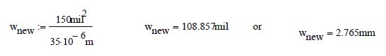
Use a 3 mm track width.
The voltage drop will now be:
Area: =0.003m·35·10-6m Cross section area of a 1oz (35 micron) copper strip 3mm wide

The analog circuit will see voltage peaks of: V:= R·10A V = 0.164V
This voltage drop may be more acceptable.
The best solution though is to use two different tracks.
One for the power circuit and one for the analog circuit. A single point parallel or star point ground. The 0.16V drop in the power circuit might still not be acceptable for that circuit, but at least the analog ground is clean!

Tutorial 2: Emissions and Solutions
The story
You inherit a design. A micro-processor circuit was built. The supply had to be some length away and the circuit is supplied with unscreened cables. Close to this area is a 100MHz receiver that is receiving noisy signals. After some investigation this circuit is suspected.
Your predecessor knew that the processor circuit was going to be used close to a receiver. That is why the circuit is enclosed in a metal enclosure. There are some concerns about the lid of the enclosure because the screws are separated at a distance x and some emissions may be leaking from here.
You investigate the circuit and find that no filters or filter circuits have been used. Good decoupling was however implemented. You also see that there was a heat problem so that the PCB is mounted close to metal enclosure. A non-conductive heat pad was used and the PCB assembly is a distance h from the enclosure floor.
You are worried about the 100MHz. The processor is running at 10MHz. The receiver is sensitive at 10 times this frequency. One would have thought that the 10th harmonic of a square wave would be significantly reduced?
You are asked to do something about this set-up. The people using the receiver inform you that a 20dB “drop” should do the job.
You first suspect that (as the other guys thought) some RF might be leaking from the lid. You open the lid but the noise at the receiver does not increase a lot. In fact, taking the lid away does not make a big difference.
So you get a brain wave. It must be the power cables radiating! You immediately replace the twisted wire pair with a screened twisted pair. You have heard that you should only ground the screen at on end. You do this at the supply end, but it doesn’t seem to help much. You connect the screen to the enclosure at the uP end, but still the same. Out of desperation you connect the screen at both ends to the supply enclosure (negative) and the uP enclosure.
Instead of reducing the noise it worsened the signal to noise ratio at the receiver! This is impossible and you are perplexed.
You hire and EMC consultant and ask him/her to take you step by step through the problem and solution.
The solution
Is it possible for the circuit to emit at 100MHz?
Yes. It was established that the logic used has rise/fall times of less than 1nsec. The associated bandwidth of the noise is:
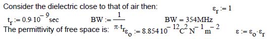
The capacitance between the PCB and enclosure is therefore:

The 20MHz clock and its harmonics also emit, but the logic edges have the higher spectrum.
Why did taking off the lid not make a significant difference?
The answer lies with the difference between common mode and differential mode emissions.
Differential mode emissions are from the loop areas on the PCB. Opening the lid let the DM emissions “out”. This is relatively small compared to emissions from the long cable sticking out of the enclosure.
Assume that the largest loop is 1cm by 1cm and that the total current flowing in these loops is 5mA. At a distance 10m away from the circuit:


13μV/m is relatively low emissions. Compare this to a typical 2mV/m that is required for good 100MHz VHF reception.
If of course the problem of the long radiating power lines is solved, the lid might become an issue if you really want absolute no interference.
Should the leakage trough the lid be an issue, keep the screws apart with not more than:


This is the lambda over 20 rule for apertures. In this case screws 150mm apart would degrade the enclosure screening with 20dB. So keeping the screw distances (or any aperture/hole sizes for that matter) less than say 50 – 100mm is OK.
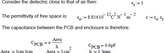
Note that the area used here is smaller than that of the physical PCB, as it will only be the area under one gate. All the other gates probably cancel each other out, as if a logic state goes high and another low, their effects cancel out

Why is the power cable emitting?
Common mode currents are generated by the switching logic. To get a feel for this consider the following:
The board and the bottom of the enclosure is acting like a capacitor. This capacitance can be calculated by knowing the area and separation h.
The above shows that there is around 0.6pF of capacitance between the PCB and enclosure.
Approximate the inductance of the wire by using 1.5nH per mm. Twice the lenght of the distance l is used (there and back)

The common mode loop will have an impedance of say:
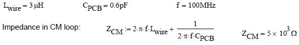
A typical common mode current will flow:

At a distance of 10m, the CM emissions will be:

This is much higher than the Differential Mode Emissions.
Why did the cable shielding not work?
Grounding the cable at only one end is typically done for analog and audio noise below 1MHz. At 100MHz and if not grounded at both ends, the shield will act like a monopole antenna.
When the shield was grounded at both ends, there were long pigtails. The pigtails (at about 1.5nH per mm) will resonate with any capacitance. This includes PCB to enclosure capacitance and stray capacitance between the cable and earth. If a resonance of this LC circuit is around 100MHz, the cable will emit even better than before.
What is the practical solution?
Three solutions. Use them on their own. Combinations will work better though.
- Use a complete shielded cable. Terminate the shield 360( with proper back shells on the connectors. If all RF current carrying circuits and connections are tightly screened/shielded, the emissions will be reduced. Depending on the frequency – good screening can give you a good 60dB and more.
- Use capacitors to chassis or other types of feed through filters at the entry point. This will dump or short the CM current to chassis (enclosure). There are different types and sizes available. 40 to 60dB of noise current reduction is possible.
- This is an easy one. Soft ferrites work very well at 100MHz. You even get them in the ‘clip-on’ variety. At 100MHz a small ferrite bead can add a few hundred ohms of resistance to the CM noise current. If you wind the wire through the bead a few times, this can go up to kilo-ohms.

IDC Technologies EMC “SG” Practical Kit
1. Contents of Kit
Radio in Shielded Box
| 1. | Grundig Mini World 100 PE Radio (Modified Antenna). | If radio with antenna is enclosed in box- no reception |
| 2. | Aluminium Gray Enclosure | Hole for feeding trough antenna wires and grounding on bare surface |
| 3. | 6 X 40 Screwdriver | For opening/closing of box |
| 4. | Green Antenna Wire | |
| 5. | Black antenna wire with feedtrough capacitive filter | To demonstrate filtering |
| 6. | Yellow/Green wire ground connection | To demonstrate that shielding or filtering effectiveness is reduced if this ground wire is used |
| 7. | Cable sleeve in plastic pipe | Use end to directly ground or connect ground wire |
SDS 200 USB Oscilloscope
| 8. | SoftDSP SDS 200MHz 5GS/s Oscilloscope | |
| 9. | USB cable for SDS 200 | |
| 10. | SoftSCOPE software (original and updates) for SDS 200 | |
| 11. | 2 off 10X Cat I/300V Probes | |
Antennae and Probes
| 12. | Telescopic antenna | Use as E-field antenna/probe |
| 13. | RG58 type current loop | Use as H-field antenna/probe |
| 14. | RG58 1.0m BNC lead | To connect antenna and sniffer probe |
| 15. | Custom build near field magnetic sniffer probe (female BNC) | High discrimination probe |
| 16. | Microsafe Microwave Oven field meter | To illustrate diode demodulation. See diode & meter trough back. Use next to cell phone. |
Switch mode PSU & Filter
| 17. | Artesyn DC-DC converter, load and filter board | Show the effects of X-capacitor, Y-capacitors and common mode choke by selecting jumpers |
| 18. | BNC to Croc-clip ground strap | Grounding of DC-DC converter/filter assembly |
| 19. | 2 off 9V batteries | |
Ferrites, Filters, Cables and Shielding Samples
| 20. | D-type SCI 56-721-015 feedtrough filter | Samples |
| 21. | Miscellaneous feedtrough filters and ferrite beads | Samples |
| 22. | Miscellaneous conductive O-ring gaskets (blue) | Samples |
| 23. | Miscellaneous samples of cables and sleeving | Samples |
| 24. | Miscellaneous samples of earth straps and copper tape | Samples |
| 25. | Miscellaneous samples of EMC gaskets material and finger stock | Samples |
| 26. | MSFC 13K Clip-on ferrite | For Current probe and/or antenna suppression |
| 27. | Yellow/white ferrite toroid and wires | To demonstrate common mode choke construction |
NOTE:
Before performing demonstrations – ensure batteries for the radio (2 X 1.5V penlight) and PSU (2 X 9V ‘522’) are ‘fresh’.
2. Radio in a Box
Place tuned FM radio with antenna in box. Close lid. No reception. Draw antenna wire from hole – reception resumes. This illustrates how emissions will take place from enclosure with UNFILTERED conductors/cables. Figure 1.
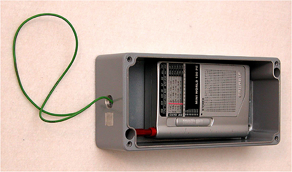
Use feed-trough filter to attenuate reception. Ground the bulkhead/feedtrough filter directly to the enclosure chassis. This illustrates the use of feedtrough filters when feeding cables trough a shielded enclosure/faraday cage boundary. Figure 2
Use the earth wire to ground the filter. The filter efficiency reduces (does not work). This illustrates that there is too much impedance for FM reception (around 100MHz) in a round wire. It also illustrates how filters can be ineffective – i.e. bad grounding. At 100MHz a round wire cannot be used as bonding/grounding. Figure 3.

With the box closed, feed the antennal wire through the cable shield/braid. If the braid is not grounded to the enclosure, nothing happens. Ground the shield to the open connective part of the box. Reception is attenuated. Figure 4.
Use the round “earth” wire to ground the shield. This does not work and illustrates that the wire is not a good conductor at FM frequencies. It also illustrates why pigtails on cable screens diminishes the shielding effectiveness – Figure 5.

NOTE:
Before performing demonstrations – ensure batteries for the radio (2 X 1.5V penlight) and PSU (2 X 9V ‘522’) are ‘fresh’.
3. Cell Phone Shielding
Enclose a cell phone (not included) inside the box. Tighten the screws. Contact the mobile phone. If properly shielded it should not receive the call. Note the blue EMC gasket in the lid. If it still receives, plug the large hole with metallic gauze (or steel wool). Figure 6.
Feed a wire through one of the smaller holes. Depending on signal strength, the phone should now receive an incoming call.
4. Common Mode Choke
Use the toroid and wires to illustrate the windings and working of a CM choke.

5. PSU & Filter
Use the jumpers on the PSU filter to show effects of different filter elements. Red WIMA is Cx. Two black C’s are Y-caps. Use the ground extension strap to connect PSU plane to scope. This will accentuate CM effects. Jumpers closest to input selects CM choke. Figure 8.

6. Microwave Oven Safety Meter
Use a cell phone (operating around 800 – 900MHz) to transmit and measure at the antenna with the microwave oven meter (Figure 9). Through the back of the meter (Figure 10) a diode/crystal can be seen connected directly to the meter. This illustrates demodulation of RF by a diode.
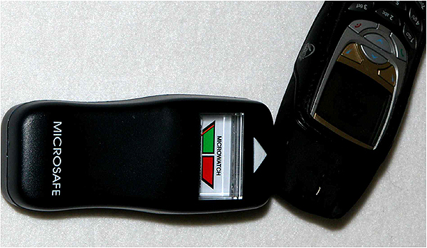
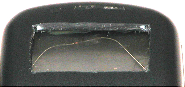
7. List of Demonstrations
| Description | Relevant Chapter(s) | |
|---|---|---|
| 1. | Use radio on FM and/or AM to receive noise from PC, projector, PSU’s, dimmers, cell phones – anything in the lecture room. Show that the noise radiates form cables! | 2 & 3 |
| 2. | Measure the emissions of a cell phone (GSM 900MHz) using the microwave leakage detector. The levels are shown as ‘dangerous’. | 4 |
| 3. | Shield the radio in the box. Antenna wire inside & outside. Open & close the lid. Try with a cell phone. | 4 |
| 4. | Show samples of gaskets and finger stock. | 4 |
| 5. | Demonstrate the shielding of the radio antenna with the cable braid. If the cable shield/braid is not grounded it doesn’t work. | 4 & 6 |
| 6. | Show different samples of braid and/or flat copper/tinned strips. Explain why round wires have high impedance at RF and why flat, large area connections work well for bonding. | 5 |
| 7. | Demonstrate that using a pigtail on the braid is not effective. | 5 & 6 |
| 8. | Use the microwave leakage detector to show demodulation of RF by a nonlinear element – the diode can be seen through the back of the detector. | 7 |
| 9. | Use the feed-through filter, radio and box to show how a conductor entering an enclosure should be filtered to chassis (the box). | 4 & 8 |
| 10. | Show that using a pigtail reduce the effectiveness of the feedtrough filter. | 4 & 8 |
| 11. | Illustrate the wiring and working of a CM choke using 2 wires and a toroid core. | 8 |
| 12. | Show samples of clip-on ferrites, ferrite beads and feedtrough filters (single and D-type) | 8 |
| 13. | Show how a loop on the scope probe pick up noise. | 9 |
| 14. | Use the PSU set-up to show how CM noise presents itself as DM noise on the scope (CM to DM conversion). Measure somewhere on the DC-DC with the scope probe & crocodile clip shorted. Make sure there is a CM path to the scope by grounding the PSU board with the braid. | 3 & 9 |
| 15. | Clip a ferrite onto the scope leads. Use a couple of windings. This should reduce some of the CM noise on the scope. | 8 & 9 |
| 16. | Use the differential scope probe (2 probe) method for measuring DM noise in a high CM noise environment (on the DC-DC). | 9 |
| 17. | Illustrate how a co-axial current loop and telescopic antenna pick up noise. The current loop works well close to the DC-DC where there is a high magnetic field. | 9 |
| 18. | Use the high discrimination sniffer probe to detect magnetic field leakage. Sniff around the DC-DC and show where the largest magnetic fields are. Sniff across the back of a laptop and show emissions leaking at the seams. | 9 |
| 19. | Use the co-axial magnetic field probe with a clip-on ferrite as a current probe. Measure conducted emissions on the DC-DC (without the filter) or laptop supply. | 9 |
| 20. | Measure noise at the battery terminal of the PSU assembly and show the effects of the different capacitors and CM choke, by switching them in and out with the jumpers. Do this for DM and CM. | 10 |
Practical Demonstrations – Extras
8. Faraday Shield and Ferrites
Use a bag of copper mesh and a small portable radio.
Replace the antenna with a piece of wire. The wire is insulated. If the antenna makes contact with the screen it doesn’t work.
If the FM radio is dropped in the bag, it stops receiving.
It works with cell/mobile phones as well, but the cell phone is harder to silence (because of higher frequency).

If the antenna wire is taken through a hole in the mesh (shield), the radio starts working. This shows that if any conductor is passed (unfiltered) through a shield, the shielding is violated. Works with well for FM.

Use an EMI suppressing ferrite and wrap a few turns around it. If outside of the shield – reception is hampered. If the radio is in the shield but the ferrite filters the antenna breaking through the shield, it doesn’t receive – as opposed to the situation without it. Shows how good the ferrite works!
The ferrite does not have the same effect on AM reception < 2MHz. Ferrites work well around 100MHz!

9. DC-DC Converter and Common Mode Noise
Use a switch mode DC to DC converter. A small rechargeable lead-acid battery is a good supply as it will not generate any noise – as opposed to a bench supply. Load the DC-DC with resistors. A number of effects can be demonstrated:

- Use an oscilloscope and show switching noise on the input/supply side of the DC- DC. Scope on AC and a few mV resolution.
- Use an AM and/or FM radio to pick up switching noise from the supply.
- Show that the radiated noise comes from the supply side wires. The conducted noise that now emits is on the cables all the way to the supply/battery/bench supply and is not just localised around the DC-DC itself.
- Connect 1nF to say 10nF caps to all the inputs and outputs and bring the other side of the caps together. In a design these caps will be connected to chassis. Show that when the common point of the caps are connected to chassis (typically metal enclosure) of the DC-DC, the noise dies down. Illustrate with either the radio and/or the scope. The ‘chassis’ caps dump or short circuit common mode noise from the inputs/outputs to the chassis so that it does not travel along the cables.

- Connect the DC-DC input through a common mode choke. Again illustrate that the noise is reduced. A CM choke with ‘chassis’ caps on the input of the DC-DC is a very good CM filter. If the effect is not dramatic enough, use more windings and/or a larger choke.
- Since DC-DC noise is usually low, clip-on ferrites will probably not work so well but is worth a try.
Simulating Radiated Susceptibility by Bulk Current Injection
In this demonstration a home made current probe is used in reverse to inject RF onto cables.
This technique is used when it is not practical or too expensive to subject a complete system to RF illumination. Good example is an aircraft. Instead of parking a jumbo jet in a test facility chamber, RF is injected onto the cable bundles to test immunity of on-board equipment. This simulates the cables and wires acting as antennas and carrying emissions into equipment.
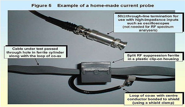
Construct a home made current/injection probe. Use a clip-on ferrite. Construct a loop antenna (magnetic near field probe) by connecting the inner conductor of a co-ax to the shield. Leave a small gap in the shield where the inner conductor was used.

This can either be used as an injection probe or current measuring probe.
For this demonstration use the probe with a signal generator and inject noise into various cables of equipment.
The following show the noise induced on a surveillance CCTV’s power leads using a signal generator around 30MHz (30Vp-p) and the home made injection probe. The two pictures are for the normal signal and noise induced signal.


Professional Certificate of Competency in Advanced TCP/IP-Based Industrial Networking
Designed for engineers and technicians who need practical knowledge in…Read more
Professional Certificate of Competency in Allen Bradley Controllogix / Logix5000 PLC Platforms
Designed for engineers and technicians who need practical knowledge in…Read more
Professional Certificate of Competency in Arc Flash Protection
Designed for engineers and technicians who work in the electrical…Read more
Professional Certificate of Competency in Chemical Engineering and Plant Design
Designed for engineers and technicians who need practical knowledge in…Read more
Professional Certificate of Competency in Circuit Breakers, Switchgear and Power Transformers
Designed for engineers and technicians who need practical knowledge regarding…Read more
Professional Certificate of Competency in Control Valve Sizing, Selection and Maintenance
Designed for engineers and technicians who need a solid understanding…Read more
Professional Certificate of Competency in Electrical Power System Fundamentals for Non Electrical Engineers
Designed for engineers and technicians who need to understand the…Read more
Professional Certificate of Competency in Electrical Power System Protection
Designed for engineers and technicians who need practical skills and…Read more")
Professional Certificate of Competency in Electrical Wiring Standards: AS/NZS 3000:2018 (Australia and New Zealand Only)
This professional development course is designed for engineers and technicians…Read more
Professional Certificate of Competency in Fundamental E & I Engineering for Oil and Gas Facilities
Designed for engineers and technicians who need to update their…Read more
Professional Certificate of Competency in Gas Turbine Engineering
Designed for engineers and technicians who need practical skills in…Read more
Professional Certificate of Competency in Hazardous Areas and Intrinsic Safety For Engineers and Technicians
Designed for engineers and technicians who need to understand the…Read more")
Professional Certificate of Competency in Heating, Ventilation and Air-Conditioning (HVAC)
Designed for engineers and technicians from a wide range of…Read more
Professional Certificate of Competency in IEC 61850 Based Substation Automation
Designed for engineers and technicians who need to understand the…Read more
Professional Certificate of Competency in Industrial Data Communications
Designed for engineers and technicians who need to understand how…Read more
Professional Certificate of Competency in Instrumentation, Automation and Process Control
Designed for engineers and technicians who need to gain practical…Read more
Professional Certificate of Competency in Machine Learning and Artificial Intelligence
This professional development course is designed for engineers and technicians…Read more
Professional Certificate of Competency in Mechanical Engineering
This professional development course is designed for engineers and technicians…Read more
Professional Certificate of Competency in Onshore and Offshore Pipeline Systems
Designed for engineers and technicians who need to gain an…Read more
Professional Certificate of Competency in Power Distribution
designed for engineers and technicians who need to gain a…Read more
Professional Certificate of Competency in Practical Machine Learning Using Python for Engineers and Technicians
Designed to use Python Programming to work with machine learning…Read more
Professional Certificate of Competency in Practical Python for Engineers and Technicians
Designed for engineers and technicians who need to understand the…Read more & SCADA Systems")
Professional Certificate of Competency in Programmable Logic Controllers (PLCs) & SCADA Systems
Designed for engineers and technicians who need to get practical…Read more
Professional Certificate of Competency in Project Management for Engineers & Technicians
This professional development course is designed for engineers and technicians…Read more
Professional Certificate of Competency in Safety Instrumentation Systems for Process Industries
Professional development course designed for engineers and technicians who want…Read more
Professional Certificate of Competency in Sewage and Effluent Treatment Technologies
Designed for engineers and technicians who need practical skills and…Read more
Professional Certificate of Competency in Structural Design for Non Structural Engineers
Professional development course designed for engineers and technicians who need…Read more")
Professional Certificate of Competency in Substation Design (Main Equipment)
Professional development course is designed for engineers and technicians who…Read more")
Professional Certificate of Competency in Substation Design (Control, Protection and Facility Planning)
Designed for engineers and technicians who need to gain practical…Read more
Professional Certificate of Competency in the Fundamentals of Process Plant Layout & Piping Design
Professional development course is designed for engineers and technicians who…Read more
Professional Certificate of Competency in Practical Mechanical Sealing
This professional development course is designed for engineers and technicians…Read more
Professional Certificate of Competency in Road Construction
This professional development course is designed for engineers and technicians…Read more
Professional Certificate of Competency in Specification and Technical Writing
Master the art of writing clear, accurate, and professional technical…Read more
Professional Certificate of Competency in Hydraulics and Pneumatics
Overview of all aspects related to the construction, design, operation,…Read more
Professional Certificate of Competency in Big Data and Analytics in Electricity Grids
This course explores the use of big data & data…Read more
Professional Certificate of Competency in Renewable Energy Systems
This course covers various renewable energy systems that are popular…Read more
Professional Certificate of Competency in Smart Grids
A smart grid is an electricity network that uses digital…Read more
Professional Certificate of Competency in Hydrogen Energy – Production, Delivery, Storage and Use
Hydrogen energy short course designed for engineers and professionals interested…Read more")
Professional Certificate of Competency in Building Information Modelling (BIM)
This professional development course is covering practical aspects of using…Read more
Professional Certificate of Competency in Industrial Internet of Things
Internet of Things (IoT) is the most sort after technology…Read more